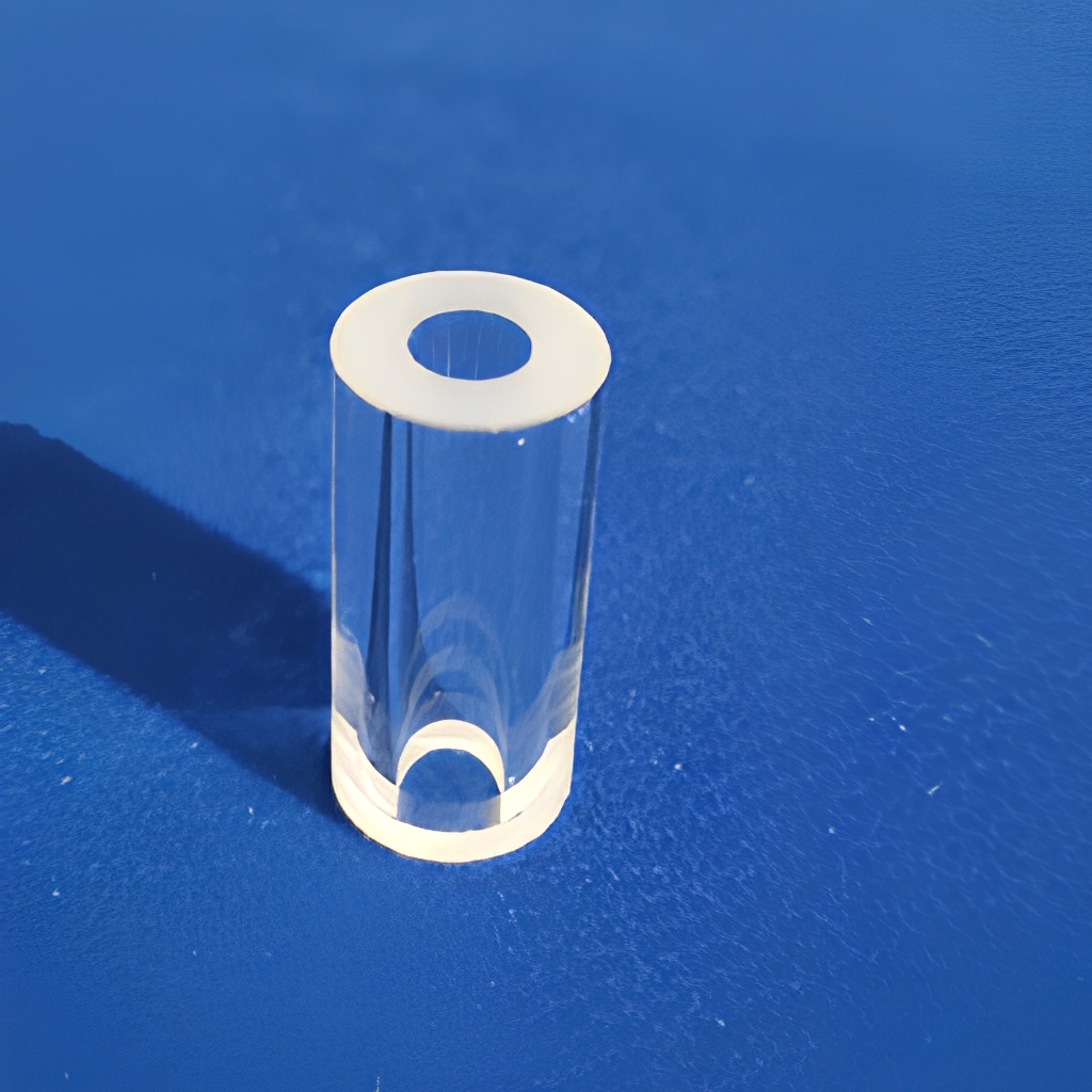
Custom Twin Geometry
99.99% Pure Clear Quartz Twin Tube
Polished, ozone-free configuration with precision customized bending, welding, and cutting designed for intensive chemical processing.
In precision photonics, semiconductor wafer processing, optoelectronics, and ultra-high-temperature chemical synthesis, the selection of an engineering material is paramount. A CE certified quartz crystal substrate supplier offers far more than raw molten silicon dioxide; certified production assures verifiable dimensional tolerances, chemical inertness, trace metal purity exceeding 99.99% (4N), and predictable structural resilience across cryogenic to 1100°C continuous thermal spectra. As microelectronics and optoelectronic assemblies downscale into sub-micron geometries, thermal expansion mismatches and particulate inclusions are unacceptable vulnerabilities. Sourcing directly from verified manufacturers with native mineral proximity provides the ultimate operational stability and cost efficiency.
SiO₂ Mineral Purity
Continuous Operating Limit
Thermal Expansion (/°C)
Engineering RFQ Turnaround
Explore eight core configurations fabricated for autoclave windows, chromatography, semiconductor furnace tubes, and high-temperature thermal barrier shields.
Polished, ozone-free configuration with precision customized bending, welding, and cutting designed for intensive chemical processing.
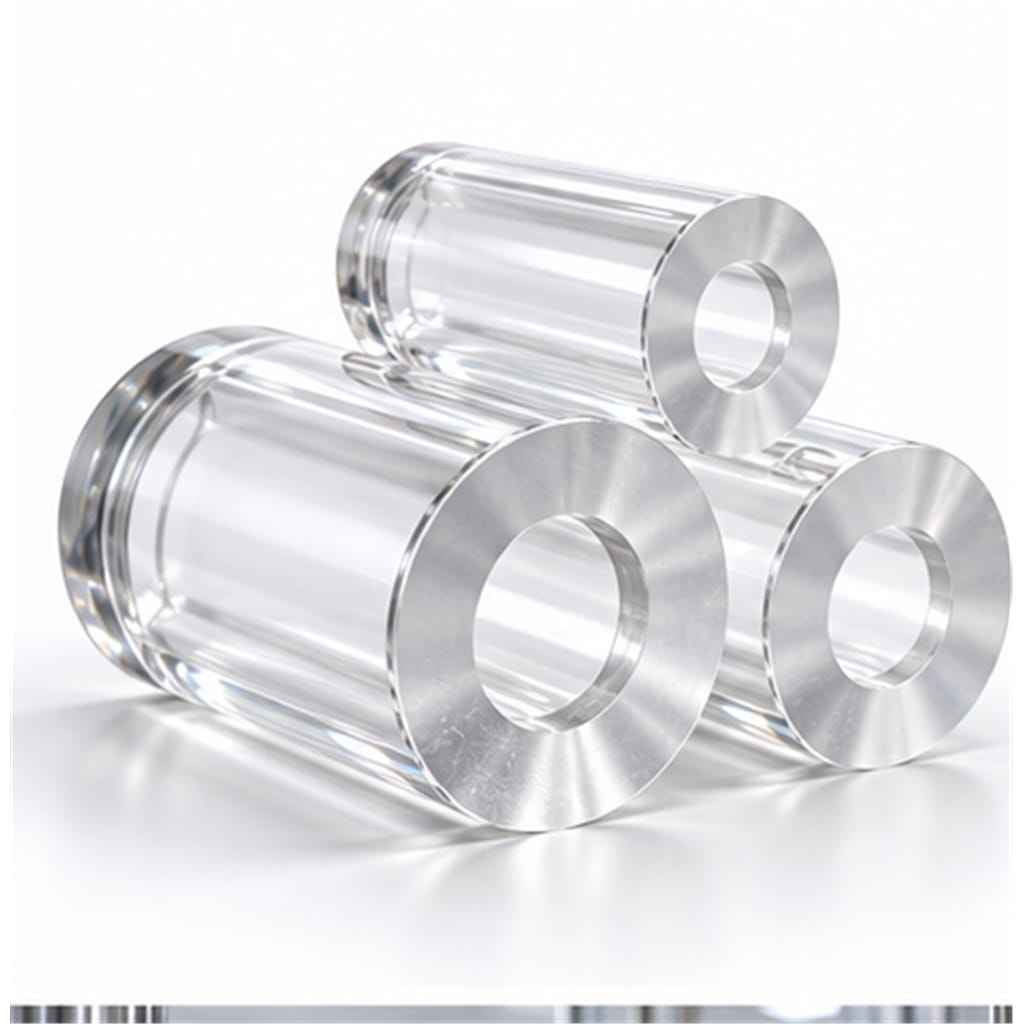
Engineered with precision-squared ends for extreme structural resilience in high-pressure autoclave sight glass installations.
Dimensionally stabilized thermal discs offering zero optical distortion, fine surface lapping, and high thermal shock tolerances.
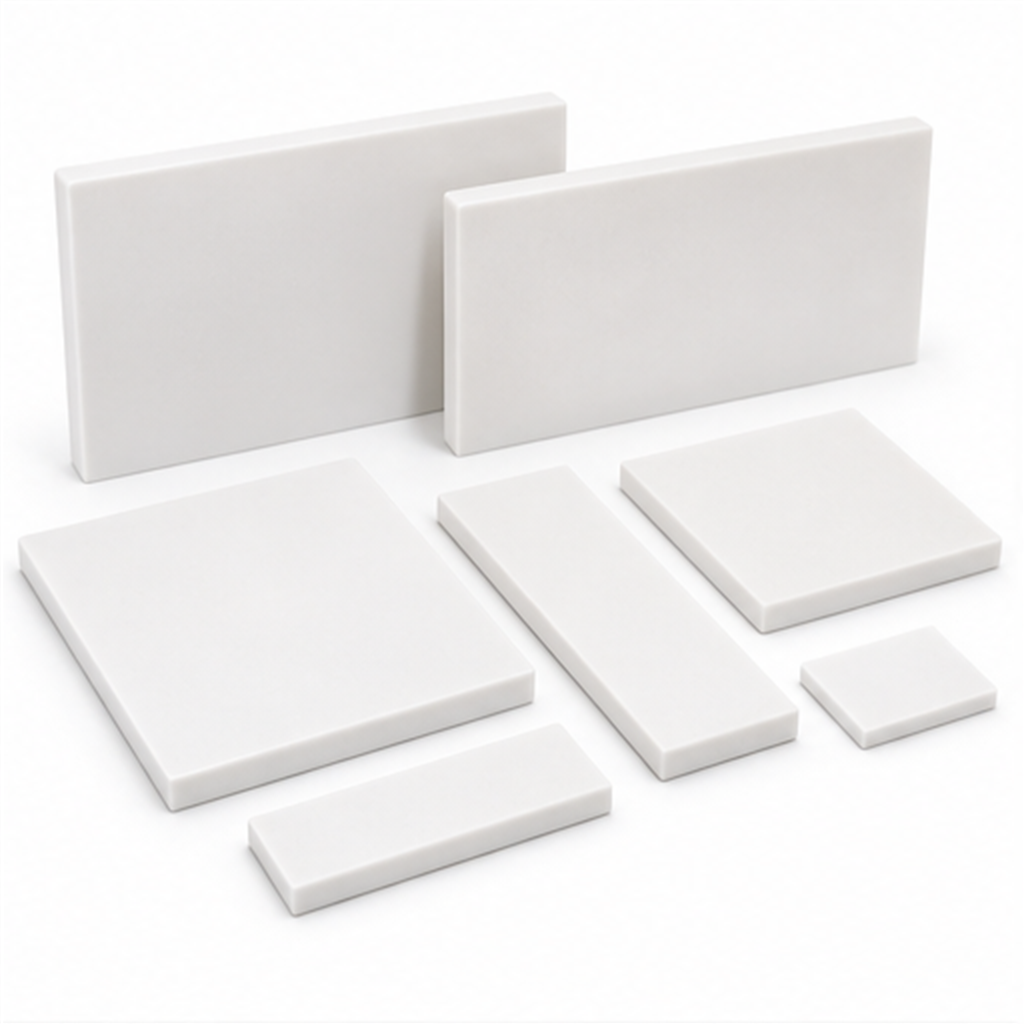
Micro-porous structure scattering infrared wavelengths efficiently for thermal barriers, furnace shielding, and flange substrates.
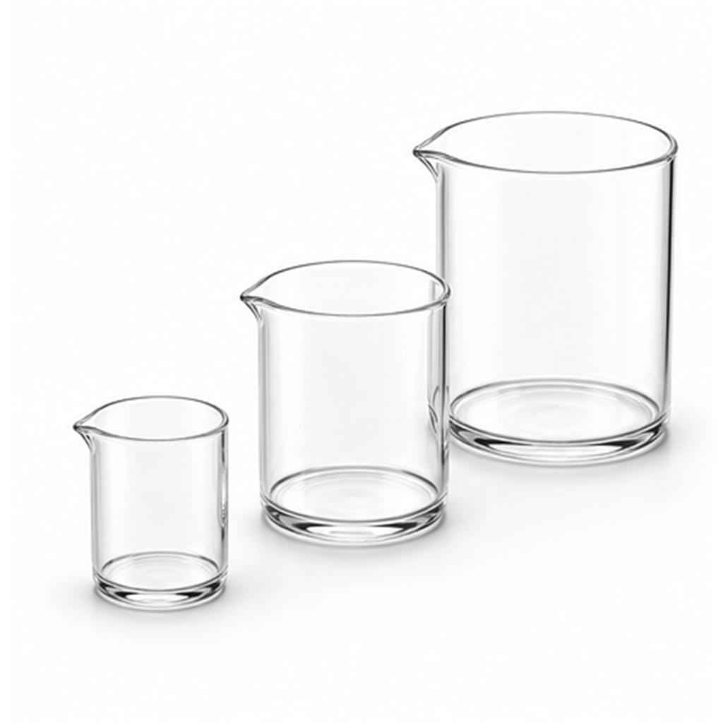
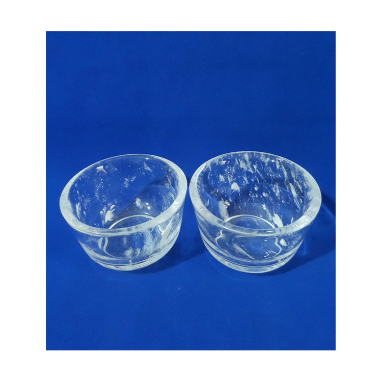
Molded pour-spout glassware with complete chemical resistance against hot acids, ideal for critical digestion and thermal analysis.
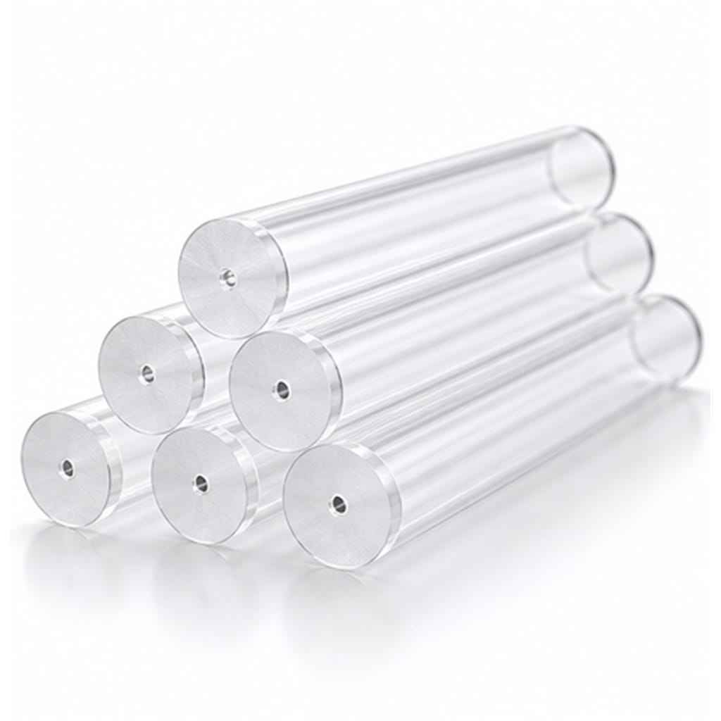
Precision micro-aperture geometry engineered for GC chromatography, electrophoresis cells, and specialized microfluidic routing.
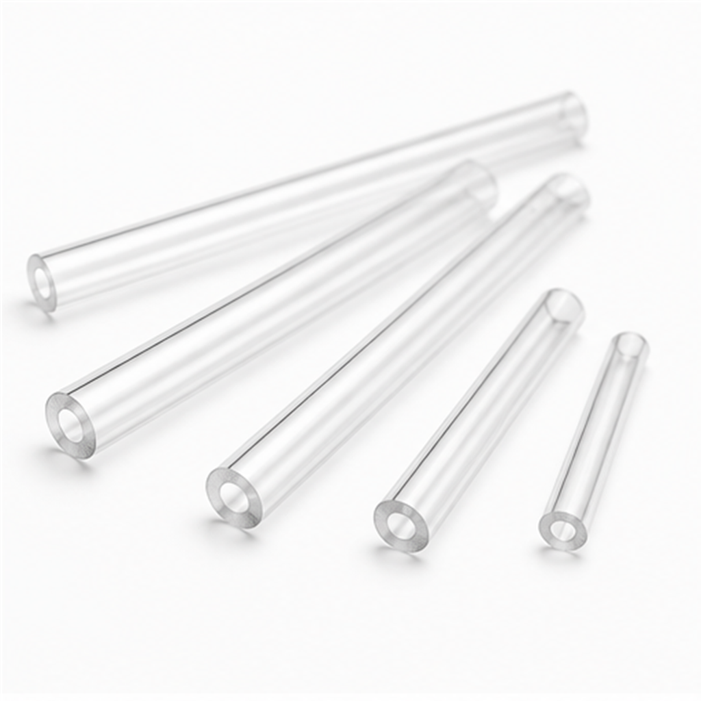
Flat-cut unpolished or fire-polished ends for seamless integration into inline spectrophotometers and analytical columns.
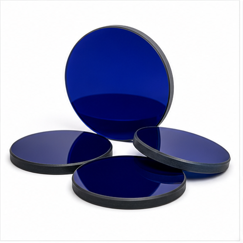
Selective spectrum furnace sight glass windows blocking dangerous flare glare while maintaining thermal integrity under continuous heat.
Understanding the atomic topography and synthesis dynamics is critical when procuring quartz substrates for mission-critical deployments. Natural fused quartz is produced through the thermal fusion of crystalline quartz sand (sourced predominantly from high-purity pegmatite geological formations). The outcome is an amorphous silicon dioxide (SiO₂ ≥ 99.99%) matrix characterized by exceptional mechanical strength, a low dielectric loss tangent across microwave frequencies, and a softening temperature of roughly 1683°C.
In contrast, synthetic fused silica is synthesized via the chemical vapor deposition (CVD) or flame hydrolysis of volatile silicon halides (e.g., SiCl₄). While synthetic silica achieves virtually zero trace metallic impurities (parts per billion level) and exhibits deep UV transmission reaching down to 185 nm, natural fused quartz remains the premier industrial choice for semiconductor wafer carriers, epitaxial tube furnaces, infrared emitters, and chemical sight viewports due to superior resistance against structural sagging at high temperatures and dramatically lower manufacturing cost structures.
| Property Parameter | Semiconductor Grade Fused Quartz | Synthetic Fused Silica | Borosilicate Glass (3.3) |
|---|---|---|---|
| SiO₂ Purity Content | ≥ 99.99% | ≥ 99.9999% | ~ 81% (with B₂O₃, Na₂O) |
| Thermal Expansion (20-300°C) | 5.5 × 10⁻⁷ /°C | 5.2 × 10⁻⁷ /°C | 33 × 10⁻⁷ /°C |
| Continuous Max Temperature | 1100 °C | 1100 °C | 450 °C |
| Softening Point (Deformation) | 1683 °C | 1600 °C | 820 °C |
| Hydrofluoric Acid Resistance | Attacked | Attacked | Rapid Etching |
| Dielectric Constant (1 MHz) | 3.75 - 3.80 | 3.80 | 4.60 |
As enterprise procurement teams navigate geopolitical supply dynamics and technical miniaturization, structural trends are redefining quartz wafer and substrate procurement:
Buyers are diversifying away from single-source raw mineral suppliers. Operating directly in Donghai County—China’s crystalline quartz hub—enables domestic security, vertical ingot melting, and insulates international supply chains from external upstream raw material embargoes.
With third-generation compound semiconductors (GaN and SiC) advancing, the demand for ultra-flat quartz carrier substrates (TTV < 2μm, Surface Roughness Ra < 0.5nm) has expanded. Double-side chemical-mechanical planarization (CMP) is now mandatory on substrate orders.
European and North American buyers require compliance with the EU Low Voltage Directive (LVD), RoHS, REACH, and Pressure Equipment Directive (PED) for high-pressure sight viewports. Audited trace analysis documents are now prerequisites prior to bill-of-lading issuance.
Traditional mechanical sawing and flame-cutting techniques are rapidly being displaced by additive and ultra-short-pulse subtractive technologies:
Sub-Picosecond Laser Micro-Machining: Femtosecond and picosecond laser drilling produces through-glass-vias (TGV) in quartz substrates with zero micro-cracking and ultra-high aspect ratios. This capability facilitates next-generation RF interposers and microfluidic diagnostic chips where thermal annealing cannot completely eliminate stresses introduced by standard diamond tooling.
Plasma Arc & Sol-Gel 3D Shaping: The convergence of pure quartz slurry 3D printing with precision sintering allows the fabrication of complex twin-tube geometries and monolithic internal cooling channels that were previously impossible to weld by hand without creating residual bubble clusters.
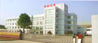
Founded in 2011 in Donghai County, Lianyungang—the crystal capital of China—Kemzo Quartz combines geographical mineral advantages with ISO 9001 certified precision manufacturing.
Essential technical, regulatory, and logistics answers for enterprise engineering and procurement specialists.
Consult directly with Donghai Kemzo’s material engineering department. Receive thorough feasibility validation, chemical purity data sheets, and competitive tiered factory pricing within one business hour.