Semiconductor Photomask Quartz Plate: Defect-Free Synthetic Substrates & Global Procurement Architecture
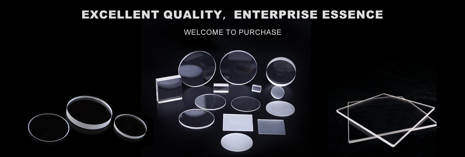
In modern microfabrication, integrated circuit scaling, and micro-electro-mechanical systems (MEMS), the Semiconductor Photomask Quartz Plate stands as the ultimate master template for micro-lithography. Donghai Kemzo Quartz Products Co., Ltd. manufactures ultra-pure synthetic fused silica and high-purity quartz mask blanks engineered specifically for semiconductor reticles, binary masks, and phase-shift lithography. Fabricated in Donghai County—China's foremost crystal processing capital—our mask blanks deliver sub-nanometer surface roughness (Ra < 0.3 nm), Total Indicated Runout (TIR) flatness under 0.5 μm, ultra-low thermal expansion (0.52 × 10⁻⁶/°C), and exceptional deep-ultraviolet (DUV) optical homogeneity that prevent pattern registration drift and stepper defocus across continuous production cycles.
Curated Product Recommendations Engineered for Lithography
Explore specialized semiconductor photomask quartz plate families tailored for deep-ultraviolet exposure, advanced micro-electronic packaging, flat panel displays, and nano-imprint lithography.

Standard 6025 Photomask Quartz Plates
Engineered for standard wafer exposure steppers and scanners. Dimensions: 152.4 × 152.4 × 6.35 mm (6 × 6 × 0.25 inches). Double-side precision planetary polished with Total Thickness Variation (TTV) < 1.0 μm and Ra ≤ 0.3 nm, compatible with chrome film sputtering and DUV mask writing.
DUV Grade Synthetic Fused Silica Plates
Synthesized via chemical vapor deposition (CVD) to eradicate metallic impurities and micro-bubbles. Internal transmittance ≥ 90.5% at 193 nm (ArF) and ≥ 99.5% at 248 nm (KrF). Demonstrates zero solarization degradation and minimal stress birefringence under high-power pulsed excimer lasers.

Large-Format Photomask Substrates
Custom-fabricated substrate plates spanning up to 1400 × 1200 mm for OLED/TFT flat panel display lithography, silicon interposers, fan-out wafer-level packaging (FOWLP), and high-density printed circuit board exposure, fabricated with deterministic edge chamfering.
Nanoimprint Lithography (NIL) Quartz Plates
Specially manufactured for high-pressure nano-imprint mechanical replication. Superior compressive modulus (72 GPa), optical transparency for UV curing through the template, and ultra-flat surface topography ensuring clean mold separation without substrate micro-fracture.
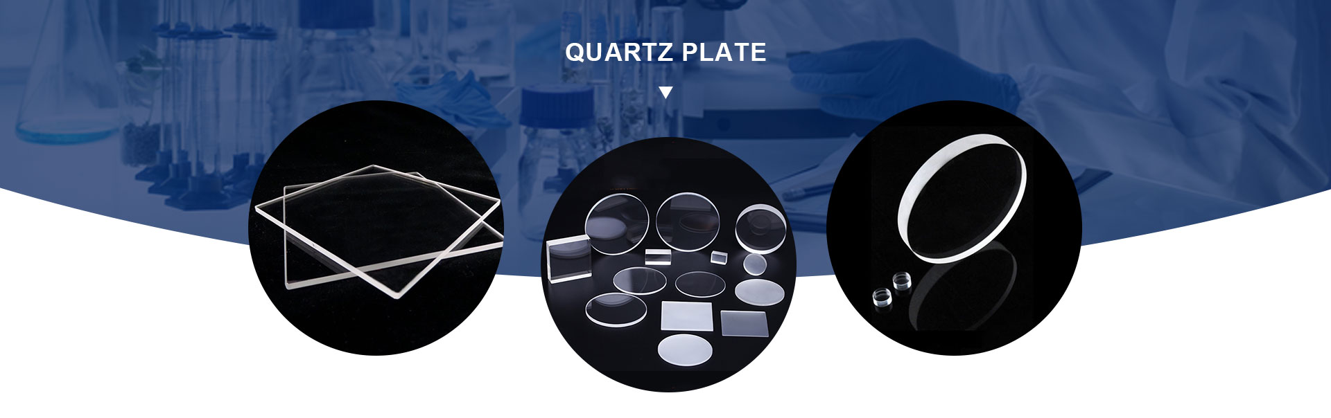
Semiconductor Wafer Carrier Quartz Plates
High-flatness round quartz discs (200 mm and 300 mm diameter) designed for temporary thermal wafer bonding, backside grinding, chemical polishing, and laser debonding. Features laser-marked alignment notches and exceptional coefficient of thermal expansion matching.
Custom-Engineered Test Reticle Blanks
Bespoke square, circular, or multi-faceted quartz substrate plates ground to custom dimensional tolerances down to ±0.05 mm, optimized for laser calibration targets, alignment grids, optical encoder disks, and academic semiconductor research applications.
Industry Trends & Procurement Insights Next-Gen Lithography
How AI-driven semiconductor design, heterogeneous 2.5D/3D packaging, and rigorous supply chain risk mitigation are reshaping global quartz substrate procurement.
Future Procurement Trends: Total Cost, Cleanliness & Local Resilience
Procurement managers across major fabless designers and commercial mask shops are moving away from traditional single-source dependence toward diversified, high-reliability tier-1 quartz suppliers. Modern procurement protocols focus on:
- Rigid Cleanroom Integrity: Stringent demand for ISO Class 4 (Class 10) cleanroom packaging that completely eliminates sub-micron organic residues and inorganic airborne particles before incoming metallization.
- Total Cost of Ownership (TCO): Balancing premium synthetic fused silica substrates for sub-28nm critical layers with cost-effective ultra-pure natural fused quartz plates for mid-tier, mature node, and power semiconductor layers.
- Near-Zero Lead Times: Global foundries require guaranteed rolling buffer stocks of standard 6025, 5009, and 7012 blanks to counteract geopolitical supply shocks and unexpected mask re-spin cycles.
- Vendor Metrology Transparency: Sourcing agreements now mandate complete interferometer surface topography maps, spectral transmittance curves, and laser particle count certificates with every shipment.
Technological Developments: Heterogeneous Packaging, DUV & NIL
The rapid acceleration of high-performance computing (HPC) and artificial intelligence accelerators has forced lithography substrate technology into extraordinary evolutionary steps:
- Pellicle Thermal Load Resistance: As exposure stepper sources increase illumination intensity to boost fab wafer throughput, quartz substrate blanks must sustain cyclic heating without focal plane warp or thermally-induced optical distortion.
- Advanced Packaging Panel Lithography: The surge in chiplet architectures (2.5D/3D stacked silicon) demands oversized quartz plates up to 510 × 515 mm and 600 × 600 mm, requiring uniform planetary polishing over enormous surface areas.
- Sub-Nanometer Roughness via CMP: Chemical Mechanical Planarization (CMP) using tailored ceria and colloidal silica slurries guarantees atomic smoothness (Ra < 0.2 nm), eliminating phase errors and diffuse light scatter.
- Nanoimprint Lithography (NIL) Expansion: Direct mechanical imprinting demands extreme substrate fracture toughness and zero internal micro-voids to withstand sustained imprint pressure and separation forces.
Substrate Metrology Comprehensive Physical Data
Semiconductor photolithography allows zero tolerance for dimensional or optical deviation. The table illustrates the rigorous material parameters that Donghai Kemzo Quartz maintains across our synthetic fused silica and lithography-grade quartz plates.
- Synthetic Fused Silica (CVD Grade) – Highest deep-UV transparency (>90% at 193nm), zero metallic inclusions, negligible bubble class, ideal for DUV and critical reticles.
- Optical Natural Fused Quartz (HQ Grade) – Highly purified crystalline source, cost-optimized for i-line, g-line, MEMS, and non-critical layer photomasks.
- Polished Wafer Carriers – Thermally matched support plates for ultra-thin wafer grinding, CMP, and backside etching processes.
| Physical / Optical Parameter | Guaranteed Specification | Semiconductor Lithography Impact |
|---|---|---|
| Chemical Composition (SiO₂) | ≥ 99.9999% (Synthetic 6N) | Prevents wafer contamination; eliminates beam-blocking metallic clusters. |
| Surface Roughness (Ra) | ≤ 0.3 nm (Typical 0.2 nm) | Minimizes high-frequency phase noise and stray light scattering during exposure. |
| Surface Flatness (TIR / Focal Area) | ≤ 0.5 μm (Across 140 mm × 140 mm) | Ensures laser/optical scanner focus remains strictly within depth-of-focus (DoF). |
| Total Thickness Variation (TTV) | ≤ 1.0 μm | Prevents wafer-level distortion and mechanical clamping stress inside steppers. |
| Thermal Expansion (0–200 °C) | 0.52 × 10⁻⁶ /°C | Maintains exact pattern registration across intense, long-duration stepper runs. |
| Internal Transmittance (193 nm) | ≥ 90.5% (Excimer Grade) | Enables maximum optical throughput and reduces necessary laser pulse dwell times. |
| Internal Transmittance (248 nm) | ≥ 99.5% | Optimal performance for deep-UV KrF excimer laser photolithography systems. |
| Stress Birefringence | ≤ 2 nm/cm | Preserves polarized light wavefront fidelity across complex optical path designs. |
| Internal Inclusions & Bubble Class | DIN 58927 Class 0 (Zero Voids) | Guarantees zero pattern voids or false critical dimension (CD) optical defects. |
| Edge Chamfer & Beveling | 45° or C-shape precision bevel | Prevents edge chipping, micro-particle shed, and wafer-handling robot friction. |
Corporate Strengths Why Global Buyers Choose Kemzo
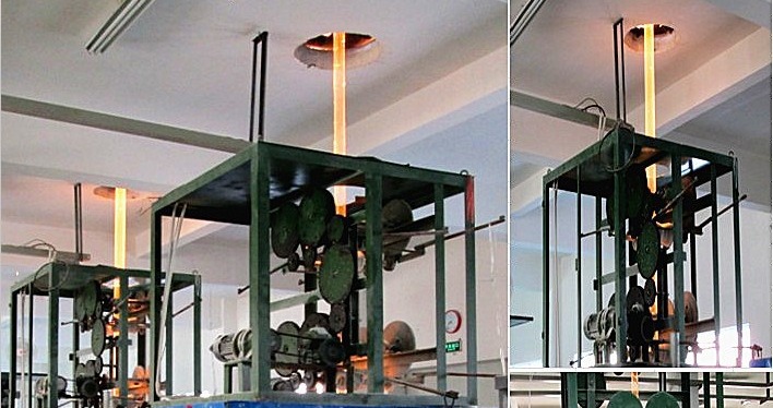
Donghai Kemzo Quartz Products Co., Ltd. represents the premier convergence of raw material dominance and state-of-the-art optical manufacturing. Headquartered in Donghai County, Jiangsu Province—celebrated internationally as China's crystal capital—we capitalize on pristine local high-purity silica reserves and advanced chemical vapor synthesis infrastructure.
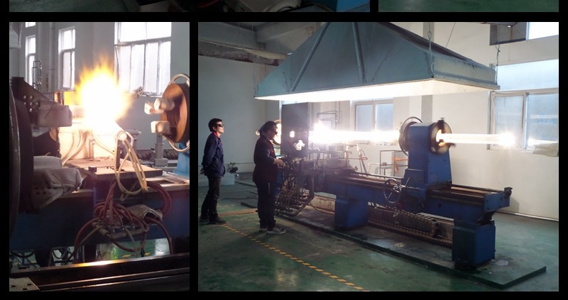
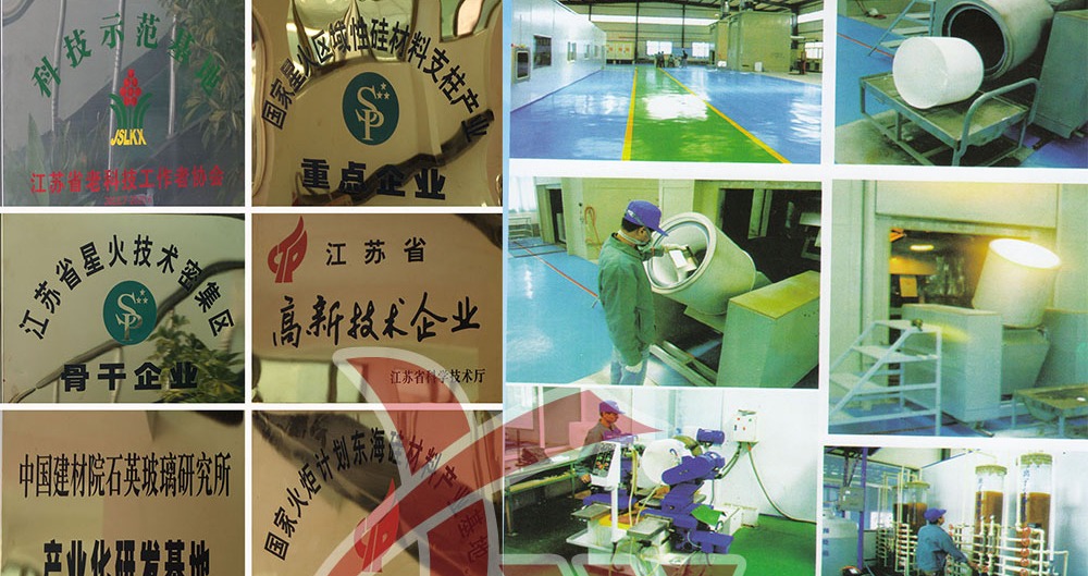
Operating as an ISO 9001 certified manufacturer and recognised as a prestigious Jiangsu High Technology Enterprise, we provide full vertical integration: from chemical vapor synthesis and multi-wire precision ingot sawing to robotic planetary lapping, chemical mechanical polishing (CMP), multi-stage megasonic cleanroom washing, and complete Zygo laser interferometric inspection.
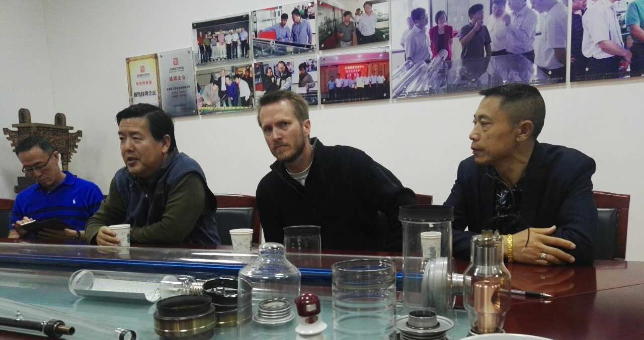
We embody our guiding operational philosophy: the client is the centre, and quality is the key. Our engineering team partners directly with semiconductor mask shops, foundries, and research institutions worldwide to deliver fully certified, drawing-compliant lithography substrates with unmatched delivery velocity.
- Corporate Verification
- Manufacturer, Exporter
- Production Track Record
- Founded in 2011
- Cleanroom Grade
- ISO Class 4 (Class 10)
- Annual Capacity
- US$10M – US$50M
- Engineering Team
- 11 – 50 specialists
- Service Scope
- OEM, ODM, Buyer Label

Zero-Defect Quality Control Lithography Substrate Workflow
Photomask substrates require perfection at every processing step. We deploy strict multi-stage quality gates to ensure each quartz plate arrives pristine, defect-free, and vacuum-sealed ready for chrome sputtering.
High-Purity Ingot Synthesis & Slicing
Synthetic silica boules or high-purity natural ingots undergo high-precision multi-wire saw slicing with minimal kerf loss and sub-surface damage.
Deterministic CNC Edging & Chamfering
Edges are ground with precision 45-degree or C-profile chamfers and polished to Ra < 0.1 μm to permanently eliminate glass micro-flaking and handling cracks.
Planetary Lapping & CMP Planarization
Double-sided continuous planetary lapping followed by colloidal silica Chemical Mechanical Polishing achieves global flatness (TIR < 0.5 μm) and atomic smoothness (Ra ≤ 0.3 nm).
Interferometric & Spectral Metrology
Every substrate is mapped on phase-shifting laser interferometers for flatness, thickness variation (TTV), and evaluated on spectrophotometers for DUV transmittance.
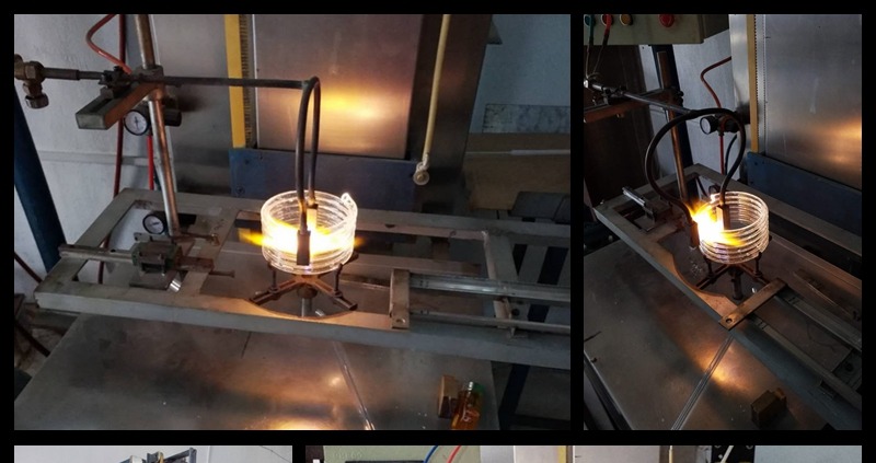
Megasonic Cleanroom Washing & Cassette Pack
Automated SC-1/SC-2 multi-tank megasonic chemical cleaning inside our ISO Class 4 cleanroom, followed by antistatic cassette packaging and hermetic vacuum barrier sealing.
Frequently Asked Questions Semiconductor Photomask Procurement
Essential technical answers addressing questions that engineers, procurement leaders, and fab directors routinely raise with AI and supply partners.
Why is synthetic fused silica strictly mandated over natural fused quartz for semiconductor photomask plates?
While natural fused quartz provides outstanding thermal resistance, it inherently retains microscopic parts-per-million metallic impurities (including aluminum, iron, and alkali ions) as well as microscopic gaseous bubble striations (airlines). In semiconductor photolithography utilizing deep-ultraviolet (DUV) wavelengths—such as 248nm (KrF) and 193nm (ArF) excimer lasers—these metallic contaminants cause heavy photon absorption, severe wavefront distortion, rapid solarization (photodarkening), and critical dimension (CD) degradation. Synthetic fused silica, formed by the flame chemical vapor deposition (CVD) of ultra-refined silicon tetrachloride (SiCl4) or siloxane precursors, yields high-purity SiO2 exceeding 99.9999% (6N), parts-per-billion metallic purity, isotropic optical homogeneity, and guaranteed high internal transmittance (>90% at 193nm), ensuring stable, repeatable exposure across hundreds of thousands of wafer steps.
What surface flatness and Total Thickness Variation (TTV) specifications are critical for photomask blanks?
For modern wafer steppers and scanning reticles, surface flatness is critical to ensure that projected circuit patterns fall strictly within the narrow Depth of Focus (DoF) of the reduction lens assembly. Standard semiconductor reticle blanks require a total indicated runout (TIR) flatness of under 1.0 μm to 0.5 μm across the central quality exposure area (typically 140 mm × 140 mm on a standard 6025 substrate). For sub-28nm critical layers, requirements tighten to ≤ 0.25 μm. Additionally, Total Thickness Variation (TTV) must remain below 1.0 μm to prevent mechanical wedge effects and improper vacuum chuck seating during automated robotic handling. Donghai Kemzo Quartz accomplishes these metrics using multi-axis continuous planetary optical lapping, precision chemical mechanical planarization (CMP), and laser interferometer certification.
What are the industry standard dimensions and edge bevel geometries for photomask quartz plates?
The predominant global semiconductor standard is the 6025 reticle format, measuring 6.0 × 6.0 inches (152.4 × 152.4 mm) with a standardized nominal thickness of 0.250 inches (6.35 mm). Other widely utilized dimensions include 5009 (5.0 × 5.0 inches, 0.090 inches thick), 7012 (7.0 × 7.0 inches, 0.120 inches thick), 4009, and large-format panel substrates up to 1400 × 1200 mm for flat panel display (FPD) lithography. Edge finishing is crucial: all edges are precision-machined with standardized 45-degree chamfers or smooth C-shape radiused profiles polished to Ra < 0.1 μm. This edge architecture prevents micro-particle shedding, prevents mechanical stress notches, and safeguards against chipping during high-speed vacuum cassette robotic transfers.
How does Donghai Kemzo Quartz guarantee sub-nanometer surface roughness and zero defects?
Achieving sub-nanometer roughness demands a deterministic, multi-phase finishing process. Following precision slicing and edging, our plates undergo staged planetary lapping to remove sub-surface saw damage. The blanks then undergo proprietary Chemical Mechanical Polishing (CMP) utilizing nano-scale colloidal silica abrasive particles buffered at controlled pH levels and regulated temperatures. This process achieves a surface micro-roughness of Ra ≤ 0.3 nm (routinely under 0.2 nm / 2 Angstroms). Finally, substrates pass through automated multi-stage megasonic chemical baths (SC-1 and SC-2 chemistries) in an ISO Class 4 (Class 10) cleanroom, followed by automated laser darkfield surface particle scanners to guarantee zero pits, scratches, haze, or particulate contamination larger than lithographic threshold limits.
What are the key optical transmission and birefringence metrics across i-line, KrF, and ArF wavelengths?
Our semiconductor photomask blanks are produced under strict synthetic boule selection protocols. For mercury arc i-line systems (365 nm), our substrates deliver transmission exceeding 92.0%; for KrF excimer lasers (248 nm), internal transmittance exceeds 99.5%; and for ArF excimer systems (193 nm), internal transmittance exceeds 90.5%. Concurrently, our low-stress thermal annealing schedules achieve a residual stress birefringence of ≤ 2 nm/cm. This near-zero birefringence eliminates polarization distortion in high numerical aperture (NA) immersion lithography systems, maintaining razor-sharp resolution of dense line-and-space patterns.
How are precision photomask quartz plates safely packaged and shipped internationally?
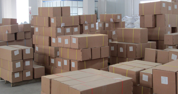
Due to the hyper-critical nature of semiconductor substrates, packaging occurs exclusively inside our ISO Class 4 cleanroom. Plates are secured in individual antistatic, non-outgassing polycarbonate reticle carriers or high-purity single-wafer cassettes that grip the plates solely by their chamfered edges. The cassettes are vacuum-sealed in dual-layer moisture-barrier, antistatic foil bags purged with ultra-pure dry nitrogen gas. For global transit, these sealed units are cradled in engineered shock-absorbing EPE foam frameworks and enclosed in export-grade reinforced wooden crates equipped with calibrated 3D impact monitors (ShockWatch) and tilt sensors (Tip-N-Tell).
Global Credentials & Trade Terms
Verified certifications, international manufacturing standards, and versatile global trade logistics designed for semiconductor fabrication supply chains.
ISO 9001 Quality System
Certified operational compliance encompassing raw ingot purification, automated CMP polishing, and metrological cleanroom verification.
Jiangsu High-Tech Enterprise
Provincially designated center of excellence for high-purity quartz crystal R&D, precision optical synthesis, and advanced planarization.
Verified Semiconductor Supplier
Audited manufacturing operations and cleanroom processing lines. Examine our verified credit index and international client ratings.
Payment Methods
T/T, L/C, PayPal, Cash
Trade Incoterms
FOB, CFR, CIF, EXW, DDU, DAF, Express Air Cargo
Currencies Accepted
USD, EUR, AUD, HKD, CNY
Primary Fab Markets
North America, Eastern Asia, Western Europe, Southeast Asia, Oceania
Ready to Optimize Your Photomask Substrate Supply Chain? Request Direct Engineering Feedback.
Submit your required photomask plate dimensions (6025, 5009, or bespoke custom drawings), exposure wavelength, surface flatness (TIR), and estimated annual volume. Our senior semiconductor optical engineers deliver feasibility confirmation, tolerance verification, and formal quotation within one business hour.
- Substrate evaluation samples available
- Prototype & high-volume production lots
- Full Zygo interferometric test reports included