High-Precision Fused Quartz Substrates & Fabrications
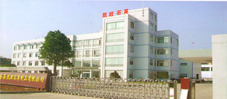
Direct from our manufacturing facility in Donghai, Jiangsu, each component meets microscopic optical, chemical, and thermal stability requirements. Available in custom dimensions, CNC micro-milled geometries, and optical double-side polished finishes.
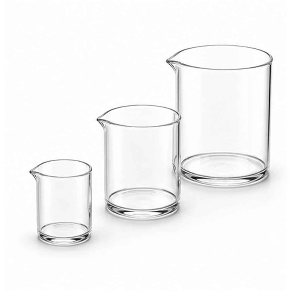
Clear Fused-Quartz Laboratory Beakers with Molded Pouring Spout for Acid-Resistant Chemical Heating
- Thermal Shock Delta T: > 1000 °C quenching tolerance
- Material Purity: Grade-A refined natural quartz crystal
- Application: Ultra-trace metal acid digestion & hot plate heating
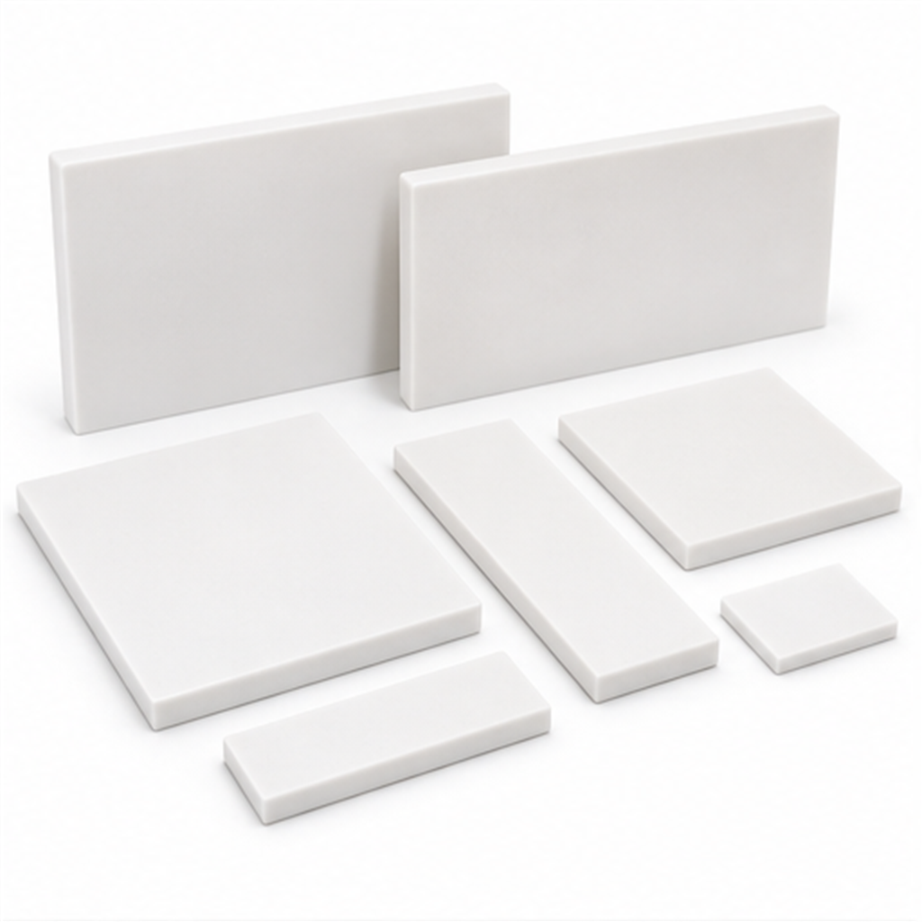
High Purity Opaque Milky White Fused Quartz Rectangular Plate Sheet Slab
- IR Attenuation: Micro-bubble light diffusion matrix
- Continuous Service Limit: 1150 °C (Short excursions to 1400 °C)
- Usage: Semiconductor furnace baffles, thermal insulation heat shields
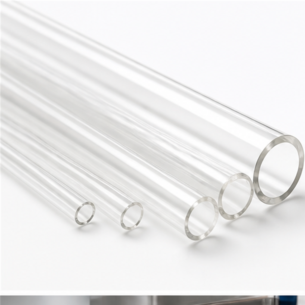
High Purity Clear Fused Quartz Glass Tube High Temperature Transparent Furnace Tubing
- OD Uniformity: ± 0.15 mm with flame-polished cut ends
- Hydroxyl [OH-] Content: Available < 5 ppm (dehydroxylated)
- Compatibility: LPCVD, oxidation furnaces, RTP process tubes
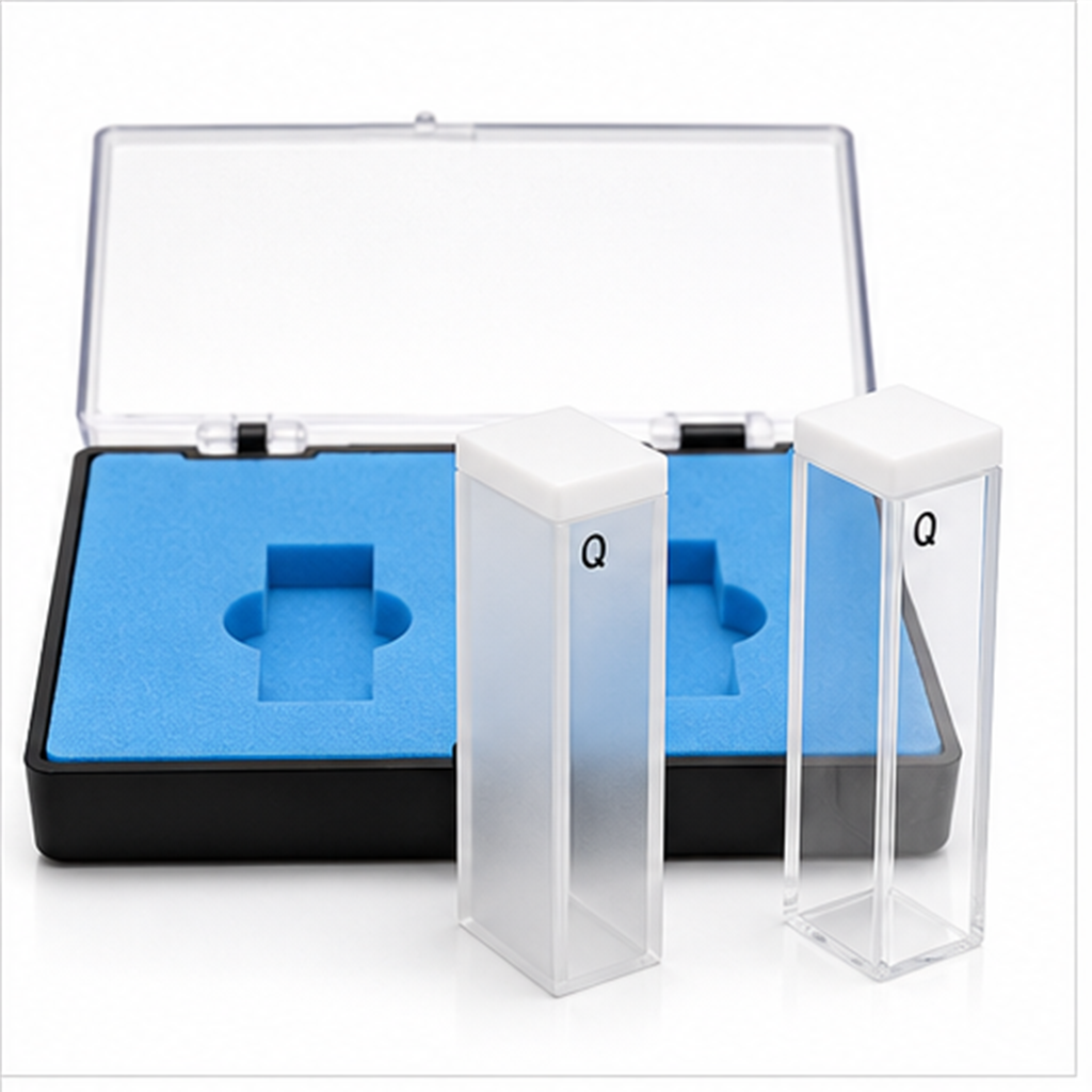
Standard 2-Window and 4-Window UV Quartz Cuvettes with Black Q Mark in Blue Foam Case
- Transmission Band: 190 nm to 2500 nm (JGS1 synthetic equivalent)
- Pathlength Precision: ± 0.01 mm with molecular fusion bonding
- Finish: Zero-glue fusion assembly resistant to acids, DMSO, acetone
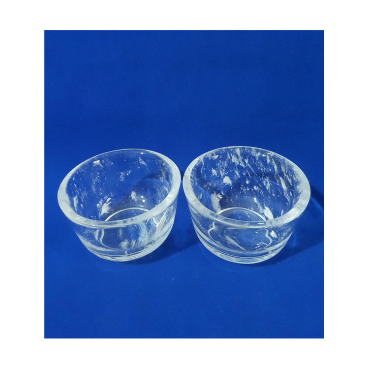
High Temperature Resistant Quartz Glass Circular Silica Custom Size Cutlery Use
- Surface Roughness: Ra < 0.5 nm CMP double-sided polish
- Thermal Expansion: 5.5 × 10⁻⁷ /°C from 20 °C to 300 °C
- Versatility: High-temp sight windows, wafer carriers, thermal setters
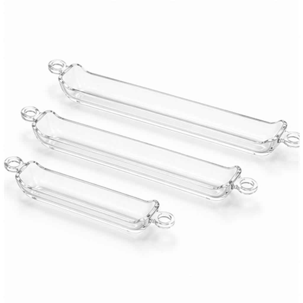
Clear Fused-Quartz Combustion Vessels with Fused Pull Rings for High-Temperature Analytical Tube Furnaces
- Joint Strength: Annealed solid quartz pull rings and heavy-wall rim
- Purity Level: Total trace metallic elements < 20 ppm
- Application: Carbon-sulfur analysis, battery powder sintering
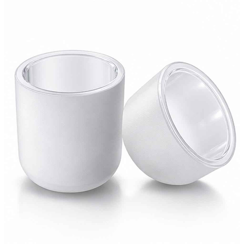
4-Inch US Sand Fused-Quartz Crucibles with Bubble-Free Inner Layer for Silicon Crystal Growth Melting
- Feedstock: High-purity silica sand (IOTA standard)
- Inner Layer: 100% micro-bubble free transparent glazed wall
- Service: Czochralski (CZ) silicon ingot pulling and compound melting
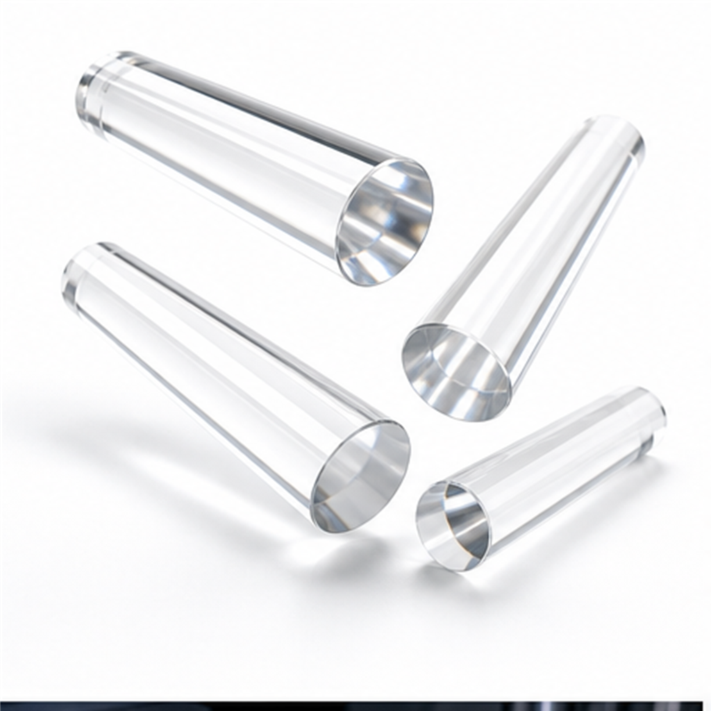
High Purity Solid Optical Clear Fused Quartz Glass Rod for Light Guide Semiconductor
- Internal Transmittance: > 92% across broadband spectrum
- Diameter Tolerance: Precision centerless ground to ± 0.02 mm
- Usage: Semiconductor wafer handling lifter pins, UV laser light pipes
Why Donghai is the Epicenter for Global Fused Quartz Engineering
Donghai County, located in Lianyungang, Jiangsu, is recognized worldwide as China's "Crystal Capital." With more than 70% of China’s natural quartz reserves and the country’s most concentrated industrial processing cluster, Donghai provides an unmatched geographic and technological foundation. Donghai Kemzo Quartz Products Co., Ltd. has leveraged this raw-material infrastructure since 2011 to establish state-of-the-art quartz refinement, hot-working, and precision machining lines.
Recognized as an official Jiangsu High Technology Enterprise and functioning strictly under an ISO 9001:2015 Quality Management System, Kemzo Quartz bridges local mineral purity with microelectronic tolerances. From chemical purity verification via Inductively Coupled Plasma Mass Spectrometry (ICP-MS) to ultra-flat double-sided Chemical-Mechanical Polishing (CMP), our operations eliminate supply chain bottlenecks for Tier-1 fabs, optical research laboratories, and photovoltaic equipment manufacturers across North America, Europe, East Asia, and Oceania.
Comprehensive Material Classification & Physical Properties Matrix
Evaluating fused quartz (melted from high-purity natural silica sand) versus synthetic fused silica (synthesized from silicon tetrachloride gas) is critical for matching dielectric, thermal, and optical performance to engineering targets.
JGS1 (Synthetic Fused Silica)
Synthesized via chemical flame hydrolysis using SiCl₄. Completely bubble-free with zero metal impurities (Fe, Al, Ti < 0.1 ppm). Exhibits deep ultraviolet transmission from 185 nm to 2500 nm without optical solarization. The premier material for excimer laser optics, lithography photomasks, and UV wafer inspection.
JGS2 (Optical Grade Fused Quartz)
Vacuum-melted from purified natural crystalline quartz crystal sand. Displays exceptional optical transparency across the visible spectrum (220 nm to 2500 nm) with remarkable structural homogeneity. The industry standard for optical viewports, sight glasses, precision prisms, and analytical spectrometer cells.
JGS3 (Infrared & Thermal Grade)
Produced via specialized electric vacuum fusion to eliminate water absorption bands. Characterized by negligible hydroxyl content ([OH-] < 2 ppm), maximizing infrared transmission up to 3500 nm. Indispensable for semiconductor furnace chambers, high-intensity infrared radiant heating, and thermal diffusion carrier plates.
| Physical / Chemical Property | Test Standard / Condition | Typical Value (Transparent Fused Quartz) | Engineering Sourcing Significance |
|---|---|---|---|
| Silicon Dioxide Purity (SiO₂) | ICP-MS / GDMS Analysis | 99.99% – 99.999% (4N to 5N) | Prevents cross-contamination in semiconductor diffusion & crystal growth. |
| Density | ASTM C693 at 20 °C | 2.201 g/cm³ | Ultra-lightweight structural substrate for precision robotic end-effectors. |
| Coefficient of Thermal Expansion (CTE) | 20 °C to 320 °C | 5.5 × 10⁻⁷ / °C (0.55 × 10⁻⁶/K) | 1/6th the expansion of borosilicate; virtually immune to thermal shock. |
| Maximum Working Temperature | Continuous Service | 1150 °C (Short duration: 1450 °C) | Maintains mechanical shape where structural technical glasses melt. |
| Softening Point | ASTM C338 | 1683 °C | Marks the absolute glass transition limit during extreme thermal surges. |
| Annealing Point | ASTM C336 | 1215 °C | Controlled thermal soak relieves stress birefringence before precision cutting. |
| Dielectric Constant (Permittivity) | 1 MHz at 25 °C | 3.75 – 3.82 | Extremely low dielectric loss; ideal for 5G/6G millimeter-wave RF substrates. |
| Refractive Index (nd) | λ = 589.3 nm (Sodium D) | 1.4585 | Uniform refractive performance for optical windows, prisms, and light guides. |
| Hydroxyl Radical ([OH-] Content) | FTIR Absorption @ 2.73 µm | Standard: < 30 ppm | Low OH: < 5 ppm | Directly governs vacuum thermal longevity and infrared optical transmission. |
Fused Quartz Substrate Sourcing Trends (2025–2030)
As semiconductor nodes scale toward sub-2nm and advanced multi-chip packaging (2.5D/3D Chiplets) expands, fused quartz and silica substrates are transforming from passive structural parts into core active process enablers.
Glass Core Substrates (GCS) for AI Packaging
Silicon and organic interposers are reaching physical limits regarding warpage and high-frequency loss. Fused quartz substrates provide superior thermal expansion match to silicon dice (CTE ~3–5 ppm) and remarkable mechanical rigidity. Sourcing teams are securing high-volume supply contracts for double-sided CMP polished quartz panels with Through-Glass Vias (TGV) for Next-Gen GPU architectures.
Extreme TTV & Sub-Nanometer Polish Standards
Procurement specifications for 200mm and 300mm quartz carrier wafers now routinely mandate Total Thickness Variation (TTV) < 1 µm, bow/warp < 10 µm, and surface micro-roughness Ra < 0.2 nm. Buyers who traditionally relied on Japanese and European manufacturers are migrating to verified Chinese suppliers capable of providing atomic-force-microscopy (AFM) verified planarization.
Dual-Sourcing & Total Cost of Ownership Optimization
Geopolitical turbulence and escalating semiconductor fab CapEx are driving procurement directors to establish resilient dual-sourcing supply chains. Partnering directly with integrated manufacturers like Kemzo Quartz—who control processing from regional quartz sand to final cleanroom-packaged wafers—cuts substrate acquisition costs by 35% to 50% without compromising GDMS purity standards.
Green Sourcing & Continuous Carbon Reduction
Traditional electric arc and oxy-hydrogen quartz melting consume extensive electrical power. Modern procurement whitepapers increasingly mandate vendor adherence to closed-loop water cooling, oxy-hydrogen flame recycling, and emission reduction standards. Kemzo continues to upgrade thermal annealers to energy-efficient electric resistance furnaces running on certified clean-grid power.
Precision Quartz Machining: From Ingot to Sub-Micron Finish
Converting ultra-hard (Mohs Hardness 7) and brittle fused silica into precision substrates requires diamond tooling, multi-axis CNC ultrasonics, and proprietary chemical-mechanical slurries.
Diamond Wire Slicing
High-speed diamond multi-wire saws slice boule ingots into wafer blanks with minimal kerf loss. This dry/wet controlled slicing process preserves the crystalline lattice boundary, eliminates deep subsurface fractures, and ensures tight starting thickness tolerances within ± 15 µm before lapping.
Ultrasonic CNC Micro-Machining
For custom holes, alignment notches, bevels, and fluidic micro-channels, ultrasonic vibration-assisted CNC spindles operate at 20–40 kHz. This reduces tool cutting pressure by 60%, completely preventing micro-cracking and chipping along edge profiles while achieving dimensional tolerances of ± 0.005 mm.
Double-Sided CMP Planarization
Chemical-Mechanical Planarization applies nanometer cerium oxide (CeO₂) or colloidal silica slurries under synchronized counter-rotating pads. This atomic-scale polishing process removes surface damage, yielding optical scratch-dig ratings of 10-5, flatness < λ/4 @ 632.8 nm, and roughness Ra < 0.3 nm.
Multi-Zone Thermal Stress Relief
After heavy CNC machining or fire-polishing, fused quartz retains internal stress that causes optical birefringence and unexpected cracking. Our programmable multi-zone furnaces perform precision thermal cycles: soaking at 1215 °C followed by slow, uniform cooling below 1050 °C, ensuring stress birefringence < 5 nm/cm.
Step-by-Step Quality Audit & Supplier Qualification Framework
International procurement managers require verified assurance before approving overseas fused quartz vendors. Kemzo Quartz follows a transparent 5-stage verification methodology designed for seamless supplier audits.
Raw Material Traceability
Every shipment is linked to specific feedstock sand batches. Mineral lots undergo glow discharge mass spectrometry (GDMS) to verify that alkali metals (Na, K, Li) remain < 1 ppm each and heavy metals (Fe, Cu, Ni) stay < 0.2 ppm, guaranteeing total thermal and electrical stability.
In-Process Laser Metrology
During drawing and grinding operations, multi-point laser gauges record OD, ID, wall thickness, and runout at 100 Hz. Data logs integrate directly with our statistical process control (SPC) system, preventing drift outside standard or custom engineering tolerances.
Interferometric Flatness & TTV
Substrates and optical discs undergo 100% laser interferometry testing using Zygo-calibrated wavefront interferometers. Total Thickness Variation (TTV), wedge angle, and surface wavefront distortion reports are generated and archived for customer traceability.
Class 100/1000 Clean Packaging
Finished substrates undergo ultrasonic deionized-water cleaning (resistivity > 18 MΩ·cm), followed by filtered nitrogen drying. Parts are heat-sealed in antistatic, vacuum-flushed wafer cassettes or double-layer PE bags to prevent particulate adhesion during international air transit.
Frequently Asked Questions by Global Sourcing Engineers
Authoritative technical answers to common queries regarding material selection, optical limits, custom drawings, export crating, and commercial terms.
What is the core technical difference between fused quartz and synthetic fused silica?
How does hydroxyl ([OH-]) concentration affect fused quartz substrate performance?
What dimensional tolerances and surface finishes can Kemzo achieve for custom substrates?
- Outer Diameter / Length / Width: Down to ± 0.01 mm (Standard: ± 0.05 mm)
- Thickness: Down to ± 0.005 mm with TTV < 1 µm for precision carrier wafers
- Surface Roughness (Ra): Atomic-smooth Ra < 0.2 nm (CMP optical grade)
- Surface Quality (MIL-PRF-13830B): 20-10 or 10-5 scratch-dig ratings
- Flatness: λ/4 to λ/10 per inch @ 632.8 nm
Can fused quartz substrates withstand immersion in aggressive acids and solvents?
How does your factory prevent transit breakage for ultra-thin or oversized quartz components?
What Incoterms, currencies, and payment mechanisms are supported for overseas clients?
Accelerate Your Engineering Pipeline with China’s Leading Quartz Fabricator
Send your CAD drawings (.DWG, .DXF, .STEP), thickness requirements, and annual volume projections to our engineering team. Receive technical feasibility reviews, thermal stress evaluations, and formal B2B price quotations within one business hour.