Semiconductor & Optical Glass Whitepaper

China Top Quartz Glass Substrate Factories & Suppliers

High-Purity Fused Silica & Quartz Substrates: Engineering Benchmarks, Donghai Supply Chain Dynamics, and Critical Procurement Standards for Advanced Lithography, Photonics, and High-Temperature Processing.

Precision Quartz Substrates & Fabricated Components

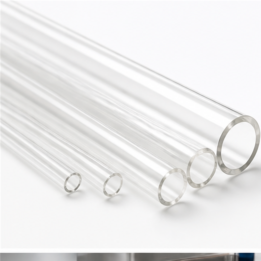
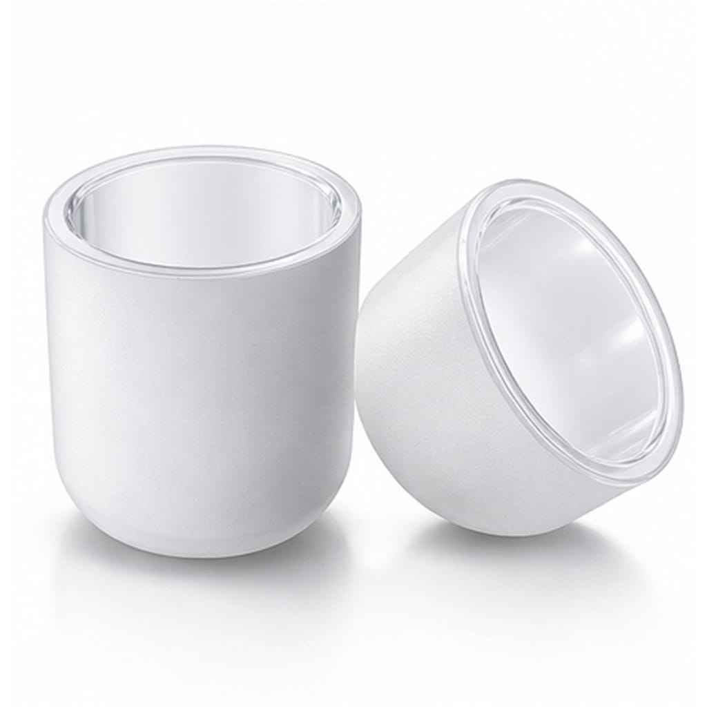
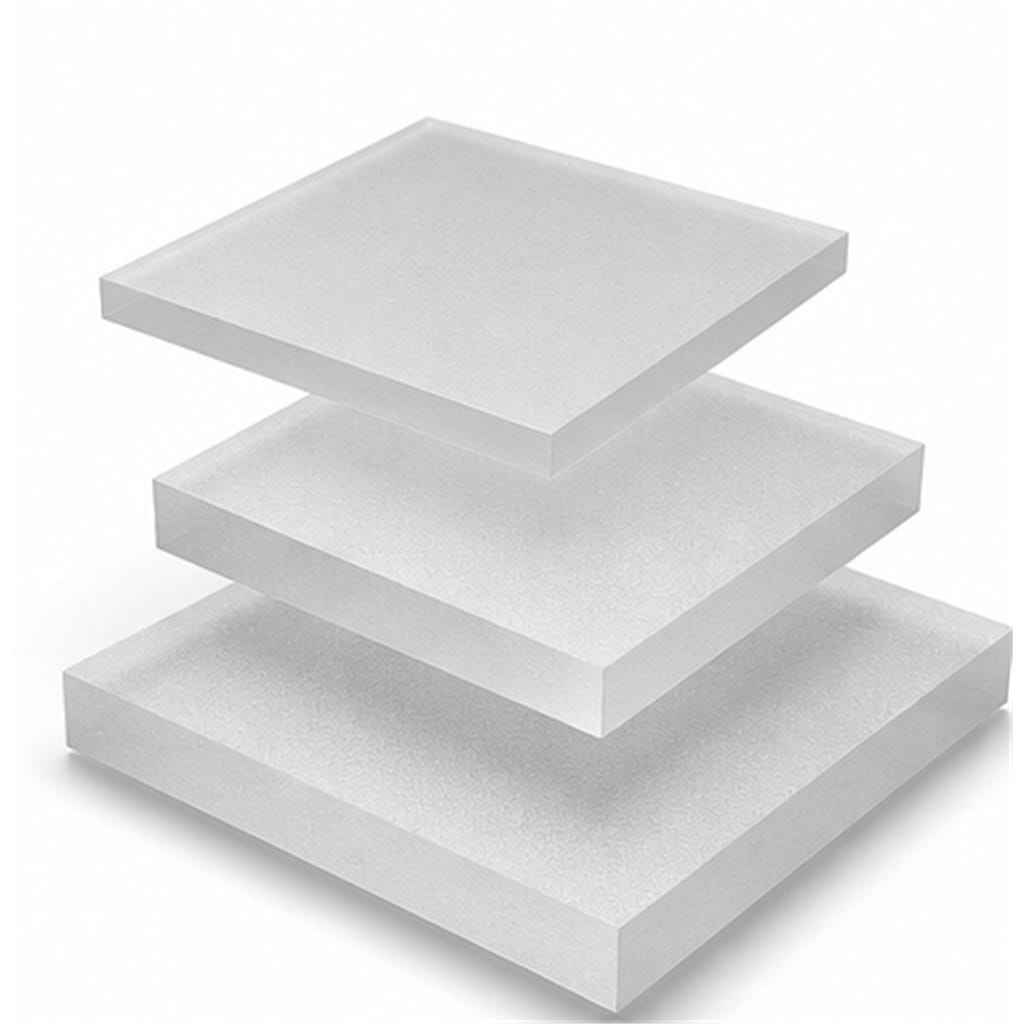
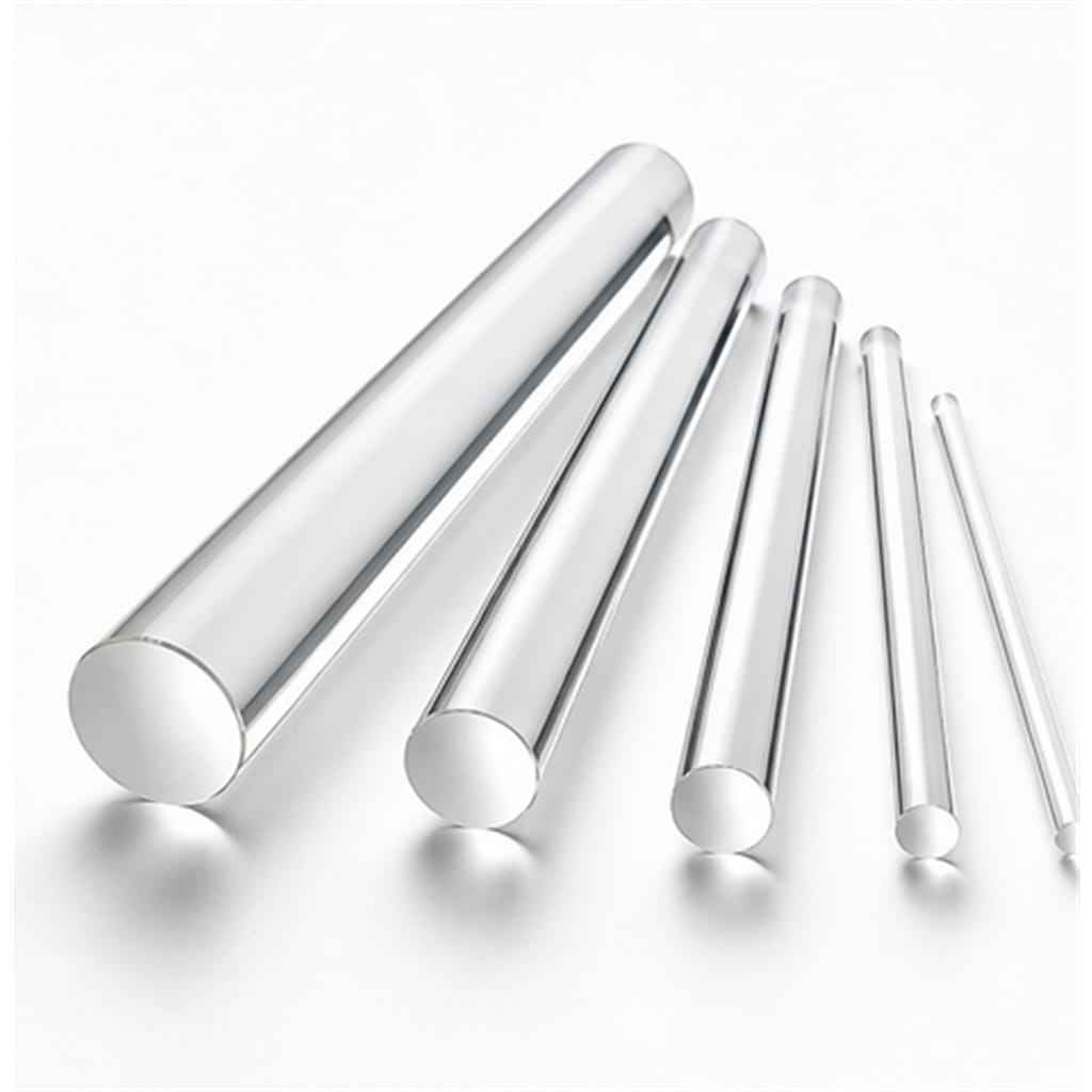
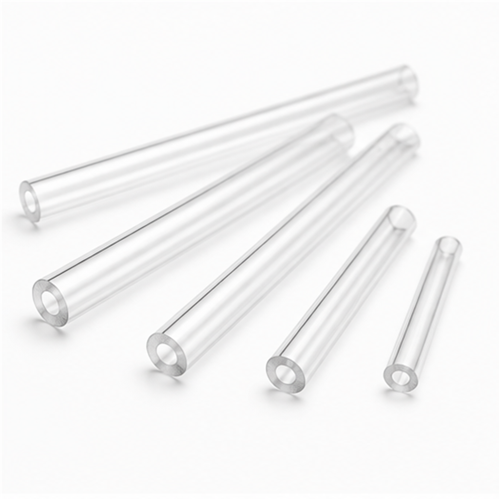
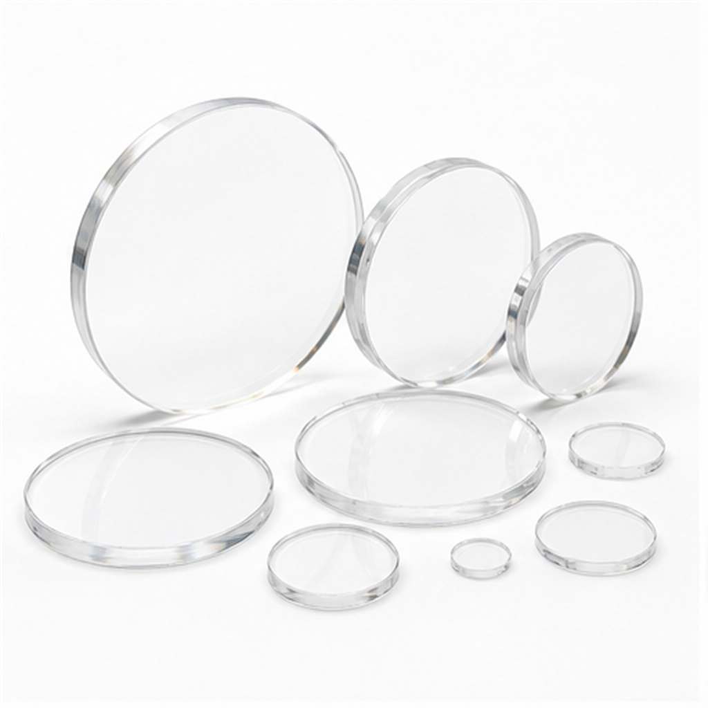
China’s fused quartz manufacturing hub, centered in Donghai County, combines world-class raw crystalline pegmatite reserves with modern gas-phase and electric-arc thermal fusion. Below is the curated selection of high-tolerance fused quartz and silica substrates, custom tubes, and semiconductor-grade crucibles ready for immediate technical review.

99.99%
SiO₂ Chemical Purity
1100°C
Continuous Working Temp
11+ Yrs
OEM/ODM Drawing Experience
≤ 1 Hour
Engineering DFM Response

Fused Quartz vs. Synthetic Fused Silica: The Procurement Decision Matrix

Procurement teams evaluating Chinese factories often conflate natural fused quartz with synthetic fused silica. While both are amorphous silicon dioxide ($SiO_2$), their crystallization pathways, hydroxyl ($OH^-$) concentrations, metallic trace profiles, and deep ultraviolet cutoffs diverge significantly. Understanding these distinctions prevents catastrophic thermal or optical failure in high-value semiconductor applications.

Property / Characteristic Natural Fused Quartz (Donghai / US Sand) Synthetic Fused Silica (CVD / VAD) Standard Technical Borosilicate
Precursor Chemistry Purified Natural Quartz Crystal Sand ($SiO_2$) Silicon Tetrachloride Vapor ($SiCl_4 + O_2$) Silica-Boron-Alkali Mix ($SiO_2-B_2O_3-Na_2O$)
Purity ($SiO_2$ Mass Fraction) 99.99% (4N) to 99.999% (5N) 99.9999% (6N) Approx. 80% to 81% $SiO_2$
Thermal Expansion (CTE: 20–300°C) $5.5 \times 10^{-7} \text{ K}^{-1}$ $5.2 \times 10^{-7} \text{ K}^{-1}$ $32.5 \times 10^{-7} \text{ K}^{-1}$ (6× Higher)
Thermal Shock Tolerance Quench from 1100°C to cold water without break Quench from 1150°C to cold water without break Fractures if rapid drop exceeds 160°C
Continuous Service Temperature 1100°C (Short peak: 1450°C) 1150°C (Short peak: 1500°C) 450°C to 500°C Maximum
Optical Spectrum Transmission 260 nm – 2500 nm (Near-UV to Mid-IR) 185 nm – 2100 nm (Deep DUV / VUV Transmissive) 350 nm – 2200 nm (Cuts off UV sharply)
Hydroxyl ($OH^-$) Content Low-OH (<5 to 30 ppm) — IR Clear High-OH (>800 to 1200 ppm) or Water-Free N/A (Multi-component glass matrix)
Typical Industrial Applications Diffusion furnace tubes, wafer carriers, RTP plates, sight windows EUV/DUV photomask blanks, excimer laser optics, TGV substrates Household glassware, low-stress lab beakers, sight glass <300°C

Trace Metal Leaching Control

In semiconductor wafer processing, trace alkali ions ($Na^+$, $K^+$, $Li^+$) and transition metals ($Fe$, $Cu$, $Ni$) cause threshold voltage shifts and minority carrier lifetime degradation. Premium Chinese factories employ dynamic thermal-acid leaching and high-frequency inductively coupled plasma mass spectrometry (ICP-MS) to guarantee aggregate impurities stay below 15 ppm.

Devitrification Dynamics

Fused quartz is a metastable glass that tends to devitrify into cristobalite when held above 1150°C in the presence of surface micro-dust or alkali salts. Controlled fire-polishing passes and ultra-clean annealing protocols seal surface micro-pores, delaying the nucleation of cristobalite phases and tripling component operational life in diffusion furnaces.

Surface Micro-Roughness (Ra/Rq)

For next-generation Glass Core Substrates and advanced packaging carriers, chemical mechanical planarization (CMP) produces atomic-level surface smoothness ($Ra < 0.2 \text{ nm}$, $Rq < 0.4 \text{ nm}$). Total Thickness Variation (TTV) is constrained to under $1.5 \text{ }\mu\text{m}$ across 200mm and 300mm wafer formats, eliminating focal shift during high-NA photolithography.

Donghai Kemzo Quartz: Vertically Integrated Manufacturing Cluster

Located in Donghai County (Lianyungang, Jiangsu)—widely recognized as China’s quartz crystal capital—Donghai Kemzo Quartz Products Co., Ltd. has specialized in the scientific melting, cold machining, and high-temperature flame finishing of fused quartz since 2011. Operating as an ISO 9001-certified entity and an accredited Jiangsu High Technology Enterprise, the facility houses over ten automated production and fabrication lines.

With raw crystalline mineral reserves right at the doorstep, the manufacturing route eliminates multi-tier intermediate sand markups, securing a consistent supply of 99.99% high-purity natural silica. Advanced 5-axis ultrasonic CNC machinery, precision multi-wire slicing saws, and cleanroom double-sided polishing beds allow Kemzo to deliver quartz substrate blanks, diffusion tubes, semiconductor boats, and optical discs adhering strictly to customer-provided CAD drawings and international SEMI standards.

Donghai Kemzo Quartz Factory Workshop

Modern High-Purity Quartz Workshop

Thermal fusion drawing towers, cleanroom polishing labs, and rigorous annealing ovens in Donghai County, Jiangsu, China.

Rigorous 5-Stage Zero-Defect Metrology Framework

Quartz substrates subjected to thermal shock or optical vacuum environments cannot tolerate internal bubbles, airlines, or micro-cracks. Chinese top-tier manufacturers enforce verifiable quality inspection protocols at every processing juncture.

Stage 1: Ingot Feedstock Assay

Incoming natural crystalline quartz rock and fused ingots undergo spectrographic analysis. Inductively coupled plasma atomic emission spectroscopy (ICP-AES) verifies total metallic impurities remain under 15–20 ppm, ensuring zero contamination ingress during subsequent thermal cycles.

Stage 2: Stress Birefringence Polarimetry

Residual internal stresses from high-temperature pulling or flame machining induce optical distortion and catastrophic cleavage under mechanical loading. Every substrate is measured with dual-polarizer stress polarimeters to ensure optical retardation stays below 5 nm/cm.

Stage 3: Interferometric Wavefront Analysis

Laser-interferometer testing (Zygo-type Fizeau metrology at 632.8 nm) verifies surface figure accuracy (PV and RMS) alongside Total Thickness Variation (TTV), Bow, and Warp across semiconductor quartz carrier discs and optical viewports.

Technological Trajectories Reshaping Global Quartz Procurement

Accelerating semiconductor chiplet integration, high-numerical-aperture EUV lithography, and high-power industrial photonics are transforming quartz glass from a standard furnace consumable into a mission-critical functional substrate.

01

Through-Glass Via (TGV) Substrate Revolution

As traditional organic silicon packaging reaches physical thermal and electrical limits, glass core substrates are ascending. Advanced Chinese suppliers are partnering with laser-induced deep etching (LIDE) developers to provide ultra-flat synthetic fused silica blanks with micro-vias down to 10–20 micron diameters, providing superior high-frequency dielectric performance for AI compute engines.

02

Large-Diameter 300mm & 450mm Thermal Tooling

Fab expansion worldwide has created massive demand for oversized, ultra-thick quartz furnace components. Monolithic quartz diffusion tubes exceeding 400 mm in diameter and precision-slotted 300 mm wafer boats require precision robotic gas-burner lathes to prevent sagging, thermal unevenness, and premature stress-corrosion fractures.

03

Green Direct Hydrogen-Oxygen Plasma Melting

Environmental compliance and energy-reduction regulations are driving Chinese Tier-1 quartz processors to transition from coal-gas flame melting to closed-loop, zero-emission hydrogen-oxygen plasma arc reactors. This shift drastically lowers bubble and hydroxyl defect rates while guaranteeing stable multi-ton volume exports without supply disruptions.

Frequently Asked Questions by Industrial Sourcing Teams

Key engineering and commercial considerations when auditing and purchasing custom quartz glass substrates and components from Chinese manufacturers.

How do natural fused quartz and synthetic fused silica compare for laser optics and semiconductor substrates?
Natural fused quartz is synthesized by electric or flame fusion of natural quartz pegmatite sand ($SiO_2$). It is highly cost-effective and provides unmatched mechanical rigidity and thermal stability up to 1100°C continuous, making it ideal for diffusion tubes, wafer carriers, furnace viewports, and general optics. Synthetic fused silica is created via the chemical vapor deposition (CVD) of gas precursors ($SiCl_4$). It delivers near-zero trace metal contamination, exceptional transmittance in the deep ultraviolet band (193 nm and 248 nm), and virtually zero bubble/inclusion presence, making it mandatory for high-NA lithography photomasks, excimer laser windows, and advanced TGV packaging.
What dimensional tolerances can Kemzo achieve on custom CNC quartz machining?
Kemzo utilizes 5-axis ultrasonic CNC centers, surface grinding, and double-side planetary CMP polishers. Standard machining tolerances for outer diameters (OD), cut lengths, and widths are ±0.05 mm, with precision optical-grade finishing achieving ±0.01 mm on request. For circular window substrates and wafer carriers, Total Thickness Variation (TTV) can be maintained under 2 microns, with parallelism under 10 arcseconds and surface flatness up to $\lambda/4$ per inch at 632.8 nm.
Why is Donghai County the central cluster for quartz sourcing in China?
Donghai County, located in Lianyungang, Jiangsu Province, is known globally as China's "Crystal Capital." It possesses the nation's highest concentration of high-purity natural quartz mineral deposits alongside the most complete industrial cluster for mineral washing, flotation refining, thermal fusion, mechanical cold working, and precision fire-working. Procuring directly from Donghai factories like Kemzo provides direct raw material supply security, shorter manufacturing turnaround, and 20–35% cost efficiency over re-distributors.
How are fragile quartz tubes, plates, and crucibles packed for international ocean and air freight?
Export shipments comply with rigorous drop-test and vibration packaging standards. Every individual quartz piece is sealed in dust-free PE wrapping, isolated with custom high-density molded EPE (expandable polyethylene) foam, and secured inside thick multi-wall inner cartons. Tubes are suspended on internal core shock absorbers so surfaces never touch. Master shipments are enclosed within ISPM-15 compliant fumigated wooden crates reinforced with steel corner bands and external impact-tilt sensor indicators.
What chemical resistances and etching limits apply to fused quartz glass?
Fused quartz exhibits near-total chemical inertness to virtually all acids, including concentrated sulfuric ($H_2SO_4$), nitric ($HNO_3$), and hydrochloric ($HCl$) acids, even at elevated temperatures up to 300°C. The only notable chemical exceptions are hydrofluoric acid ($HF$), which rapidly dissolves silica, and hot phosphoric acid ($H_3PO_4$) above 150°C. Basic alkaline solutions (such as concentrated $NaOH$ or $KOH$) will etch fused quartz at temperatures above 60°C, so careful process control is required in wet-cleaning benches.
What international trade, payment, and export compliance terms are supported?
Kemzo supports standard international commercial terms, including FOB (Shanghai/Qingdao), CFR, CIF, EXW, DDU, and express air courier door-to-door delivery (DHL/FedEx/UPS). Accepted payment methods include wire transfer (T/T), irrevocable Letter of Credit at sight (L/C), and PayPal for prototype samples. Invoices are supported in USD, EUR, AUD, HKD, and CNY.
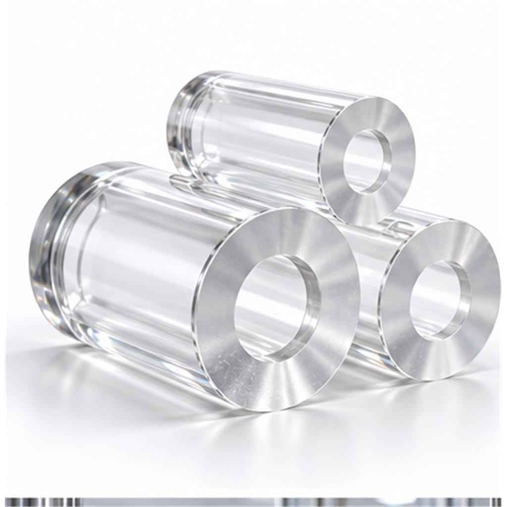
Accelerate Your Semiconductor & Optical Substrate Procurement

Submit your mechanical CAD drawings (.DWG, .DXF, .STEP, or PDF) along with operating temperature and optical tolerance requirements. Our senior glass engineers will perform a Design-for-Manufacturability (DFM) review and deliver a formal quotation within 1 hour.