High-Performance Quartz Products & Specialized Components
Manufactured to custom engineering drawings with strict tolerances. Discover our primary product offerings designed for demanding industrial, optical, and laboratory applications.
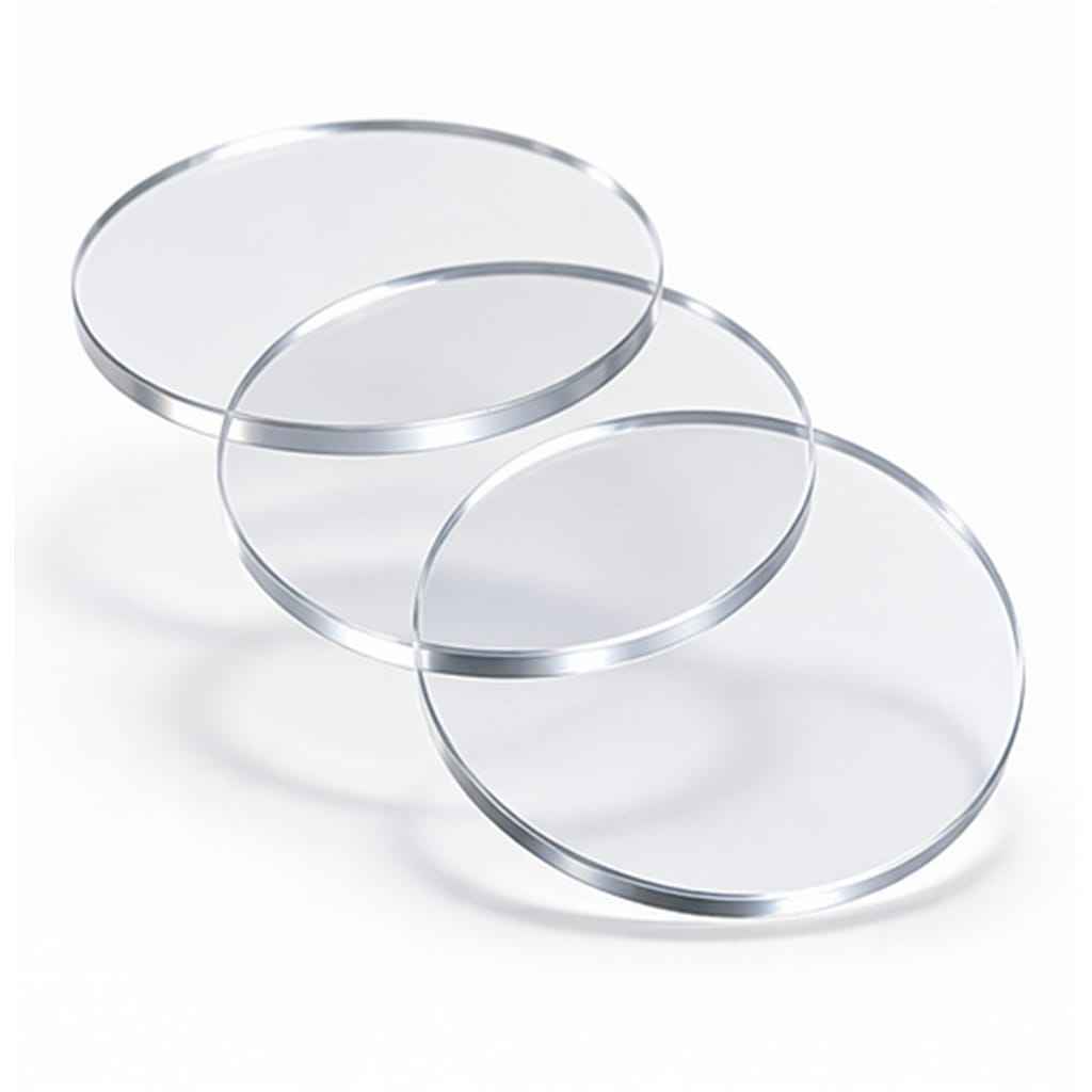
Optically Polished Single-Crystal Quartz Wafers with Chamfered Edges for Piezoelectric QCM Sensors
Ultra-flat AT-cut or SC-cut single-crystal substrates featuring fine optical polishing (Ra < 0.5nm) and precision edge chamfering to eliminate chipping in piezoelectric microbalance systems.
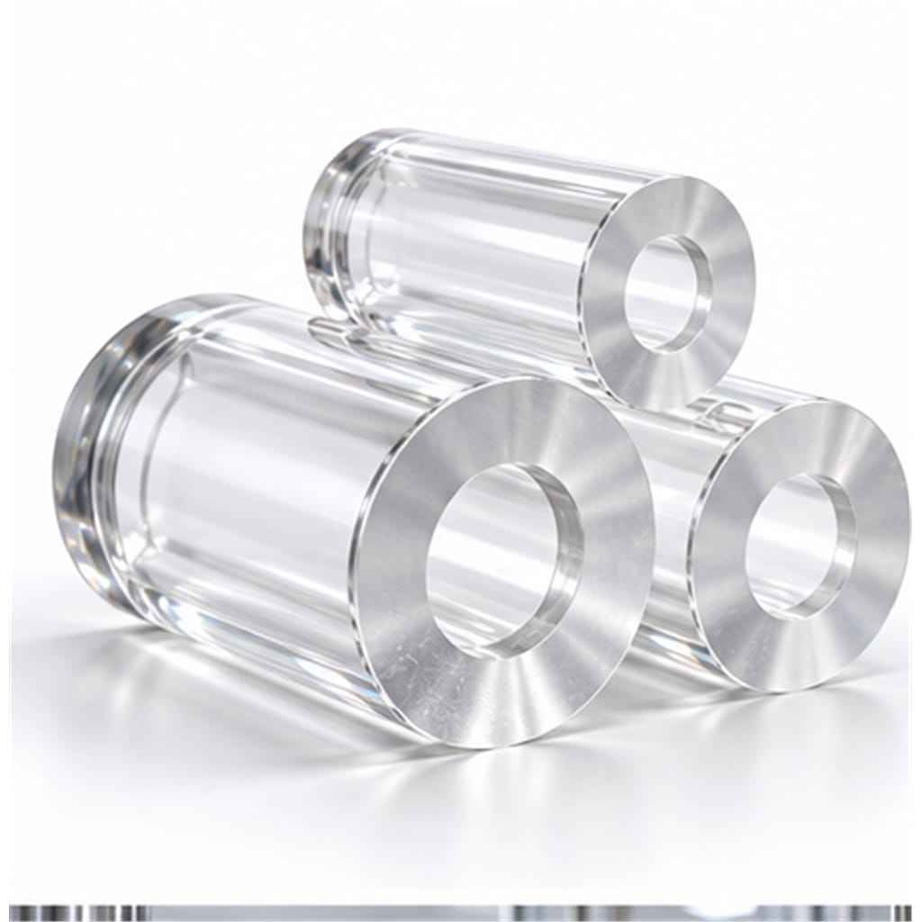
Heavy-Wall Fused-Quartz Cylindrical Pressure Tubes with Squared Ends for High-Pressure Autoclave Sight Glass
Engineered for extreme operating environments, delivering remarkable hydrostatic burst resistance, flame-polished cylindrical surfaces, and precision diamond-squared ends for leak-free sealing.
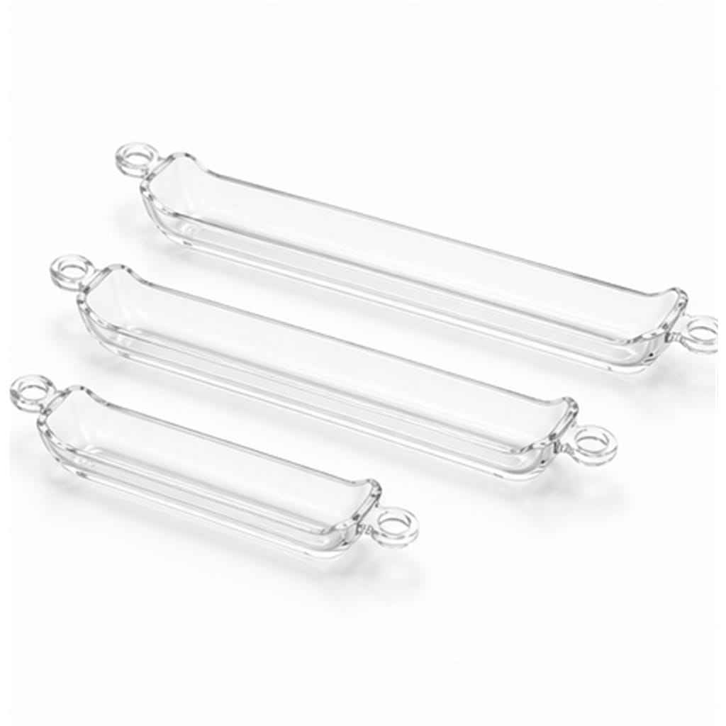
Clear Fused-Quartz Combustion Vessels with Fused Pull Rings for High-Temperature Analytical Tube Furnaces
Thermal shock-resistant combustion vessels built from semiconductor-grade fused silica. Equipped with reinforced fused rings for smooth loading and retrieval during elemental analysis at 1200°C.
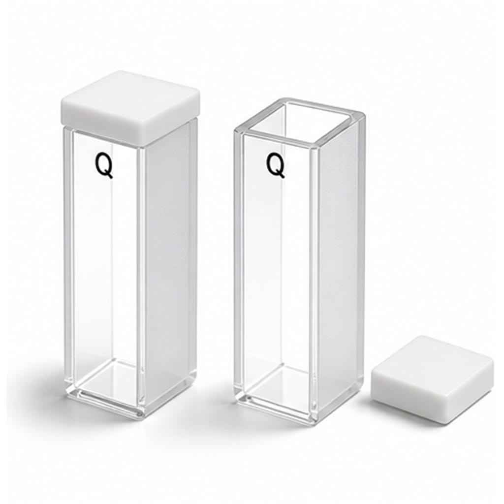
Optical Fused-Quartz Spectrophotometer Cuvettes with PTFE Lids for UV-Vis Precision Absorbance Analysis
Molecular fusion technology eliminates adhesive contamination. Offers optical transmission down to 190nm with zero bubble tolerance in the 10mm optical path for critical spectrometry.
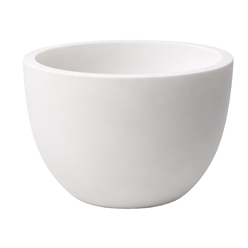
10 Inch High Purity Opaque Milky Fused Quartz Crucible for High Temp Melting Casting
Arc-fused micro-bubble milky structure delivers superior thermal insulation and uniform heat dissipation during high-purity silicon casting and precious metal metallurgy.
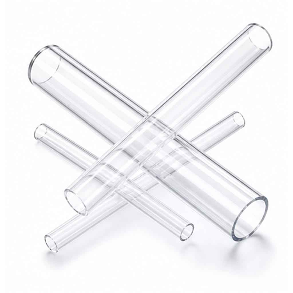
Precision Flat-Cut Fused-Quartz Straight Process Tubes with 90-Degree Squared Ends for Vacuum CVD Chambers
Heavy-gauge process tubes with controlled wall concentricity and perpendicular ends cut by diamond saws, designed for LPCVD, PECVD, and semiconductor diffusion furnaces.
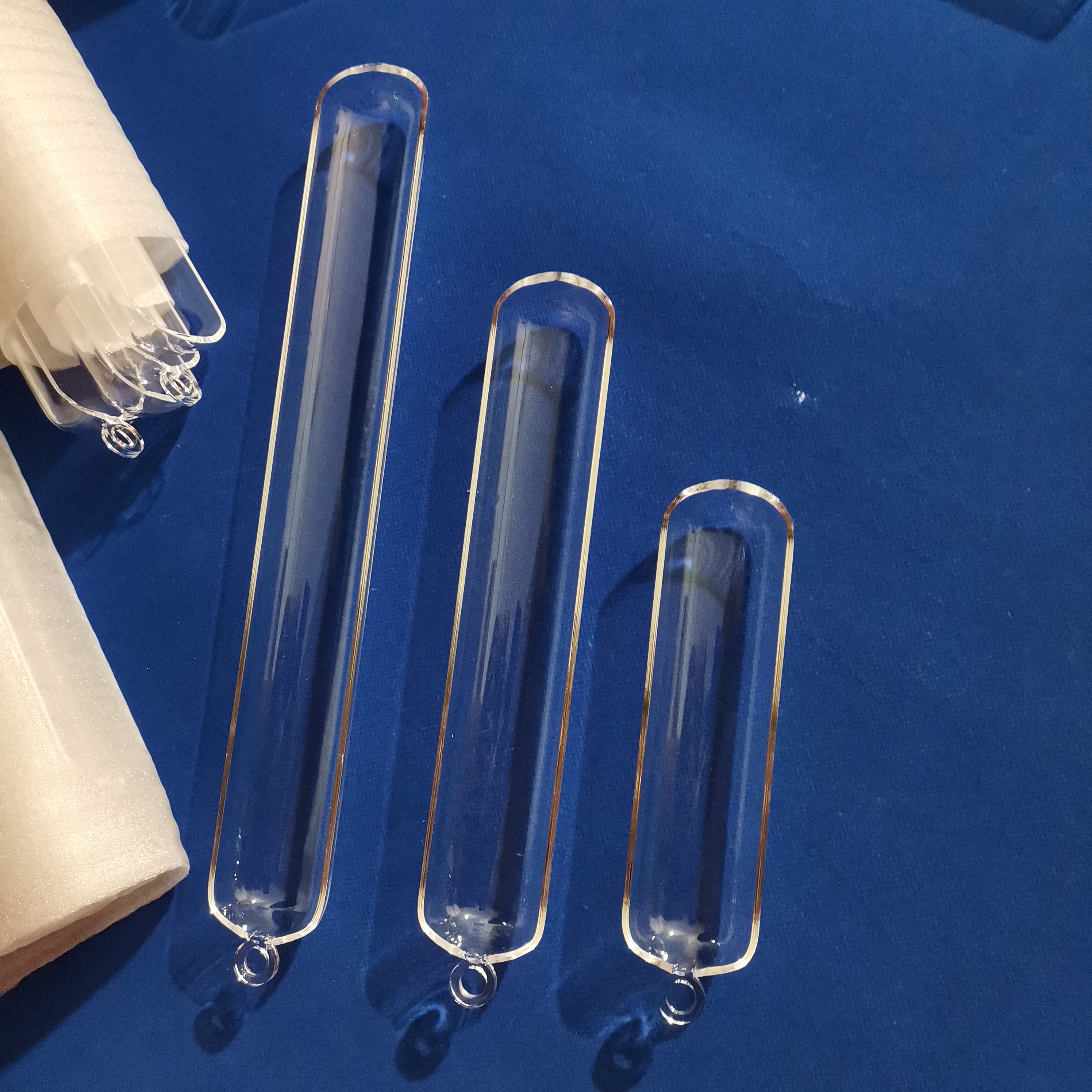
High Purity Quartz Glass Boat Transparent Bowl Shape 6-16 Chemical Industry Experimental Equipment
Acid-resistant curved quartz boats engineered for wafer carrier jigs, powder calcination, and chemical evaporation. Highly resistant to all common mineral acids except HF.
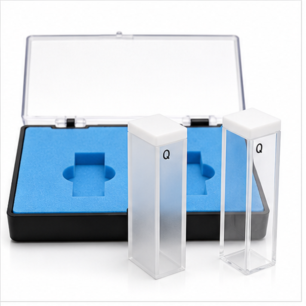
Standard 2-Window and 4-Window UV Quartz Cuvettes with Black Q Mark in Blue Foam Case
Certified spectroscopic grade optical cells featuring matched pathlength tolerance (±0.005mm). Shipped in cleanroom shockproof cases for laboratory metrology and fluorescence analysis.
Engineering Thick Fused Quartz Plates: Structural Integrity in Extreme Environments
In high-vacuum semiconductor chambers, plasma etch reactors, and high-pressure autoclave viewports, standard technical glass catastrophically fails. Thick fused quartz plates offer structural, optical, and thermal advantages.
Near-Zero Thermal Expansion
With an extremely low coefficient of thermal expansion (α ≈ 5.5 × 10⁻⁷ /°C from 20°C to 320°C), thick quartz plates undergo virtually no dimensional deformation under steep thermal gradients, remaining fracture-free even when quenched from 1000°C into cold water.
High Compressive Strength
Heavy-gauge quartz slabs (≥10mm to 100mm+ thickness) exhibit superior mechanical compressive strength exceeding 1150 MPa. This enables safe deployment in vacuum viewport flanges, deep-sea submersibles, and high-differential pressure chemical processing vessels.
Deep UV to NIR Optical Clarity
Manufactured from high-purity natural crystal sand or synthetic SiCl4, thick quartz plates retain high internal transmittance across the spectrum from 190nm deep ultraviolet through 2500nm near-infrared, unaffected by radiation-induced solarization or darkening.
| Physical / Mechanical Property | JGS1 (Synthetic Fused Silica) | JGS2 (Optical Fused Quartz) | JGS3 (Infrared Fused Quartz) |
|---|---|---|---|
| Raw Material Origin | Synthetic SiCl4 Precursor | Refined Natural Donghai Quartz | Vacuum-Melted Crystal Quartz |
| SiO2 Purity Content | ≥ 99.999% (5N) | ≥ 99.99% (4N) | ≥ 99.99% (4N) |
| Hydroxyl (OH-) Concentration | ≤ 1200 ppm (High OH) / ≤ 1 ppm (Dry) | ≤ 150 – 200 ppm | ≤ 5 ppm (Water-Free) |
| Spectral Transmission Range | 190 nm – 2200 nm (Deep UV) | 220 nm – 2500 nm (UV-Vis) | 260 nm – 3500 nm (Infrared) |
| Max Working Temp (Continuous) | 1050 °C | 1100 °C | 1150 °C |
| Annealing Point & Softening Point | 1140 °C / 1670 °C | 1215 °C / 1683 °C | 1230 °C / 1710 °C |
| Internal Bubble / Inclusion Class | DIN 58927 Class 0 (Virtually Zero) | DIN 58927 Class 1 – 2 | DIN 58927 Class 1 – 2 |
Why Tier-1 Industrial Buyers Rely on Kemzo Quartz in Donghai
Donghai Kemzo Quartz Products Co., Ltd. has established an integrated production hub in China's crystal capital, converting raw quartz deposits into high-precision heavy-wall plates, tubes, and crucibles.
Source-Region Raw Material Control
Our strategic manufacturing base in Donghai County gives us direct access to high-purity natural silica sand. Incoming quartz feedstocks undergo chemical pickling, optical sorting, and spectral mass-spectrometry checks to guarantee iron content (Fe ≤ 0.2 ppm) and total metallic trace elements below 15 ppm before melting.
Advanced Cold & Hot Processing
We combine multi-wire diamond sawing, precision CNC milling, 4-axis waterjet profiling, and double-sided planetary lapping. Thick plates up to 150mm thick and dimensions up to 1200mm × 1200mm can be ground, beveled, chamfered, and fire-polished or optical-grade double-side polished (surface roughness Ra ≤ 0.3nm).
Rigorous Quality Certifications
Operating under certified ISO 9001 protocols and recognized as a Jiangsu High Technology Enterprise, every batch undergoes polariscope thermal stress analysis, interferometric flatness testing (≤ λ/4 per 100mm), and ultrasonic thickness verification prior to export-grade hermetic packaging.
Future Procurement Trends & Technological Evolutions in Thick Quartz Plates
Global semiconductor fabs, optical lithography equipment builders, and green hydrogen electrolyzer systems are redefining performance thresholds for thick quartz products.
1. Shift to Plasma-Resistant Ultra-Pure Substrates
As semiconductor wafer fabrication advances to sub-3nm GAAFET nodes, reactive ion plasma etch (RIE) chemistry (such as CF4 and NF3) erodes standard quartz viewports, creating particulate contamination. Procurement is rapidly shifting toward synthetic dense quartz plates with zero gas inclusions and trace metal content under 0.1 ppb to maximize chamber mean-time-between-cleans (MTBC).
2. Large-Aperture Heavy Quartz for Advanced Displays
With Gen 8.6 and Gen 10.5 OLED/Micro-LED substrate processing, photolithography exposure systems require thick quartz exposure mask plates exceeding 1200mm in diagonal and 30mm to 50mm in thickness. Managing thermal distortion across massive optical apertures requires precision annealing cycles spanning hundreds of hours to lower residual birefringence below 2 nm/cm.
3. Consolidated Supply Chains via Donghai Exporters
Global original equipment manufacturers (OEMs) are consolidating procurement by partnering directly with integrated manufacturers like Kemzo Quartz. By bundling raw ingots, precision CNC milling, diamond polishing, and laser inspection within a unified industrial zone, procurement teams reduce lead times by 40% while mitigating international logistics risks.
Technological Roadmap: Edge Modification & Nanoscale Surface Planarization
Modern thick quartz plate fabrication is moving beyond mechanical lapping toward Chemical-Mechanical Planarization (CMP) and Magnetorheological Finishing (MRF). These methods eliminate subsurface micro-cracks induced during diamond sawing, increasing the mechanical fracture threshold by more than 300% under high-pressure cycle loads.
Furthermore, laser-polished chamfered edges and ultrasonic core drilling for complex bolt holes and step recesses ensure vacuum-tight seals in high-temperature CVD processing without localized thermal stress concentrations.
Frequently Asked Questions: Thick Quartz Plate Sourcing & Engineering
Technical guidance and commercial clarity for procurement managers, optical engineers, and international equipment designers.
How is the required thickness calculated for a quartz sight glass under pressure?
t = d / 2 × √( (1.06 × P × SF) / σallowable )
Where d is the unsupported diameter, P is the maximum design pressure (MPa), SF is the safety factor (typically 4 to 10 for brittle ceramic/quartz materials), and σallowable is the tensile bending strength of fused quartz (~48 MPa). For elevated temperatures (>500°C) or cycling pressure conditions, our engineering department recommends increasing thickness by 25–40% to account for thermal gradients and seal compression relaxation.
What is the difference between JGS1, JGS2, and JGS3 when ordering thick plates?
JGS2 is optical fused quartz melted from refined natural quartz crystal. It provides excellent transmission from 220nm through the visible spectrum at a more economical price point, suitable for furnace windows, observation ports, and standard optics.
JGS3 is infrared quartz melted under vacuum conditions with hydroxyl content stripped down to < 5 ppm. It eliminates the deep water absorption band at 2730nm, offering continuous transmission up to 3500nm for IR sensors and thermal imaging viewports.
Can thick quartz plates be tempered like soda-lime or borosilicate glass?
What manufacturing tolerances and surface roughness can Kemzo achieve?
How does Kemzo ensure safe transit for heavy, high-mass quartz shipments?
What export documentation, testing reports, and certifications are provided?
What are your standard payment terms, minimum order quantities (MOQ), and lead times?
• MOQ: From 1 piece for custom R&D prototypes up to full container loads for recurring OEM furnace lines.
• Lead Times: Standard sizes ship within 3–5 business days. Custom CNC machining, drilling, and double-side polishing typically require 10–18 working days.
• Incoterms: FOB, CFR, CIF, EXW, DDU, and DDP via express courier (DHL, FedEx, UPS).
• Currencies & Payment: USD, EUR, AUD, HKD, and CNY via T/T wire transfer, L/C at sight, or PayPal for sample fees.
Need Custom Thick Quartz Plates or Technical Feasibility Feedback?
Send your CAD drawings (.DWG, .DXF, .STEP, or .PDF) along with working temperature, pressure differential, and optical tolerance specifications. Our senior engineering team in Donghai will review your design and provide a detailed quotation within 1 hour.