Precision Fused Quartz & Silica Product Range
Manufactured to critical drawing tolerances for semiconductor diffusion, chemical vapor deposition (CVD), photolithography, and analytical assaying across the Kanagawa industrial base.
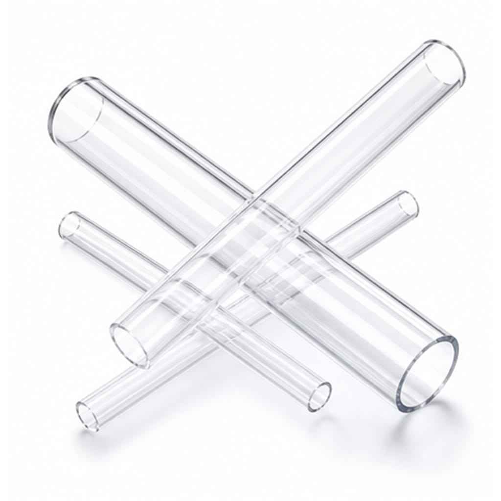
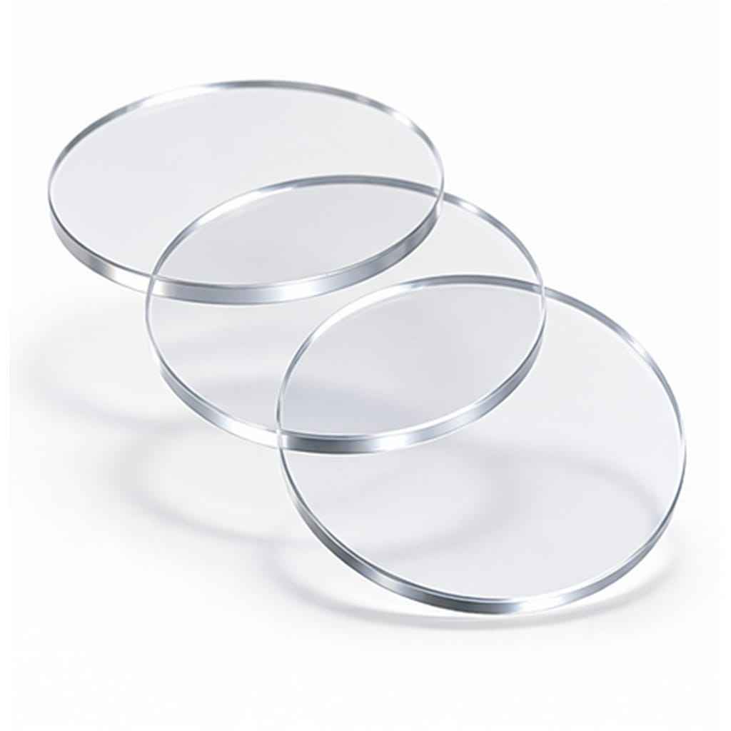

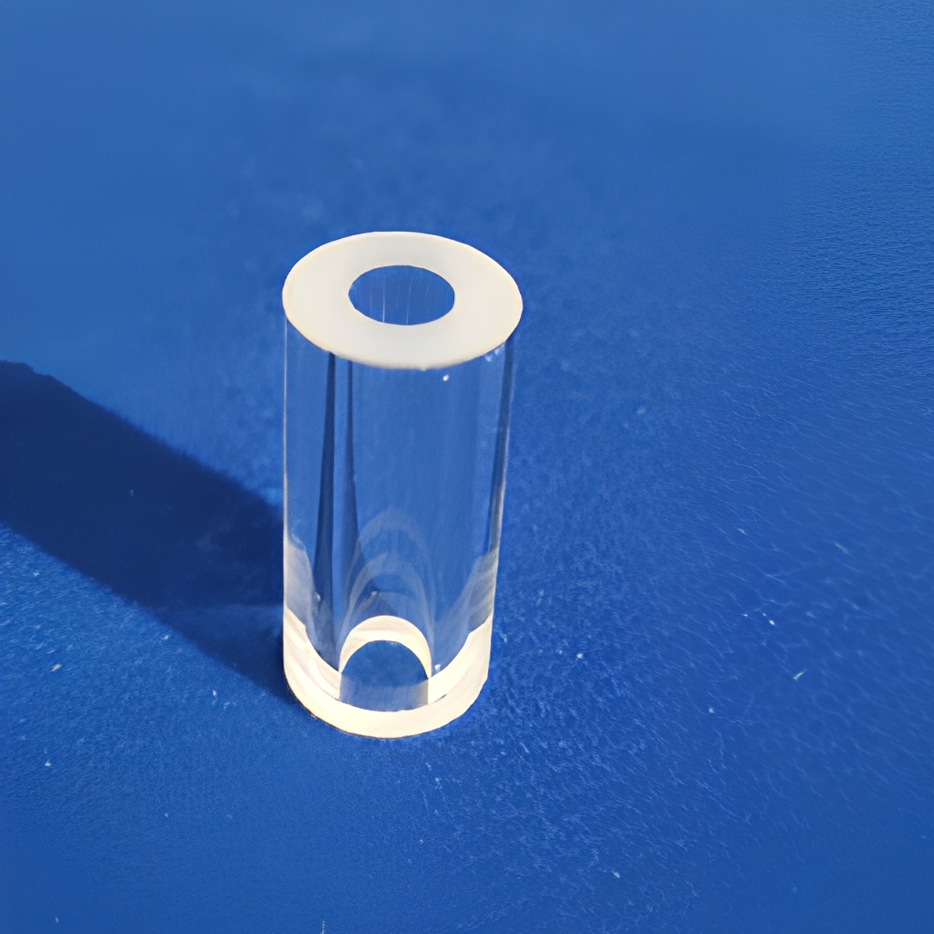
Material Science Benchmark: Fused Natural Quartz vs. Synthetic Fused Silica
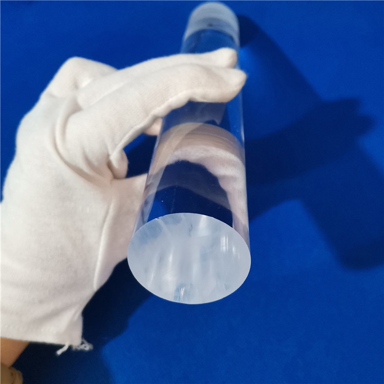
In high-precision manufacturing environments across Yokohama, Kawasaki, and the broader Keihin Industrial Zone, technical procurement leaders frequently evaluate the operational boundary between natural fused quartz (electric or gas-melted) and chemical-vapor-deposited synthetic fused silica (SiO₂ ≥ 99.999%). Natural fused quartz delivers superior mechanical creep resistance, structural rigidity at continuous operating profiles reaching 1100°C, and exceptional cost-performance for structural furnace tooling, process liners, and carrier boats.
Synthetic fused silica, formed from chlorinated silane precursors (such as SiCl₄), delivers virtually zero trace-metal inclusions (Fe, Al, Ti, Na < 0.1 ppm aggregate) and eliminates optical absorption bands in the Deep Ultraviolet (DUV) range down to 193 nm. For advanced semiconductor photolithography inspection and excimer laser optics operating along Tokyo Bay research clusters, synthetic formulations prevent solarization and refractive index drift under continuous ultraviolet irradiation.
| Thermal & Mechanical Metric | Electric Melted Clear Quartz | Synthetic Fused Silica | Significance for OEM Engineering |
|---|---|---|---|
| Operating Limit (Continuous) | 1100 °C | 950 °C - 1050 °C | Maintains structural tube roundness under thermal CVD loads. |
| Peak Limit (Short Term) | 1450 °C | 1200 °C | Permits high-rate spike anneal cycles without sagging. |
| Thermal Expansion (CTE) | 5.5 × 10⁻⁷ / °C (20–320°C) | 5.2 × 10⁻⁷ / °C | Near-zero expansion prevents thermal shock catastrophic fracturing. |
| Softening Point (Log η = 7.6) | 1683 °C | 1585 °C | Defines upper viscosity boundary for custom flame lathe processing. |
| Dielectric Strength (20°C) | 25–40 kV/mm | 35–45 kV/mm | High-voltage insulation for plasma etch electrostatic chuck systems. |
Localized Industrial Applications Across Yokohama Ecosystem
Strategic integration with Kanagawa's premier semiconductor equipment manufacturers, green hydrogen research consortiums, and photonic testing facilities.
Semiconductor Epitaxy & Diffusion
In Yokohama's Kohoku New Town and Kanagawa Science Park (KSP) corridors, microelectronics fabrication relies on our precision flat-cut quartz furnace tubes. Featuring zero hydroxyl (OH) variations and strict dimensional tolerances, these process tubes serve low-pressure LPCVD, ALD, and atmospheric diffusion furnaces, preventing trace-metal wafer contamination during multi-step gate dielectric formation.
Photovoltaic & Green Energy
Aligned with Yokohama City's Carbon Neutral Port initiative, our heavy-wall quartz reaction tubes and customized twin-tubes drive advanced perovskite-silicon tandem cell experimentation. Excellent infrared transmittance ensures uniform radiant heating, while high mechanical durability withstands continuous plasma-assisted deposition cycling without devitrification.
Chemical & Metrology Glassware
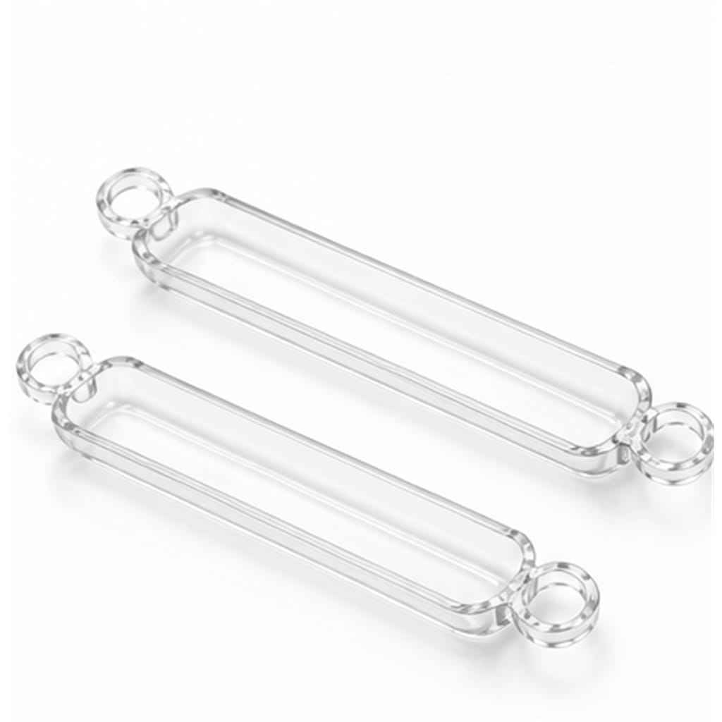
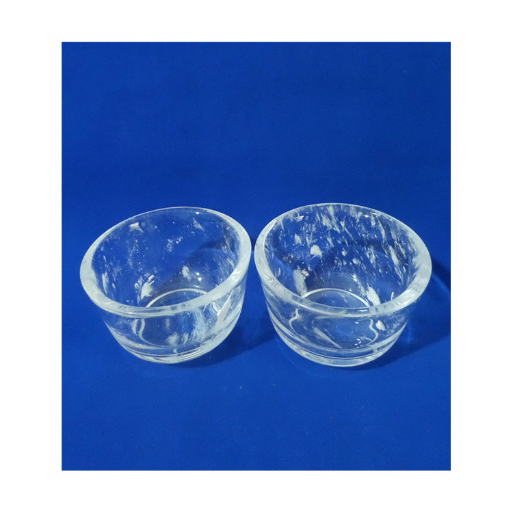
Serving industrial testing laboratories along the Tsurumi and Daikoku wharves, Kemzo supplies ground-joint vacuum adapters, combustion boats with integrated pull rings, and optical spectrophotometer cuvettes. Our clear fused quartz resists aggressive mineral acids—including boiling aqua regia, nitric acid, and sulfuric acid—ensuring zero analytical baseline drift.
Key Market Trends Reshaping Quartz Procurement in Kanagawa Prefecture
The semiconductor equipment ecosystem in Japan is experiencing an aggressive pivot toward domestic supply-chain resilience and supply security. Driven by initiatives from METI (Ministry of Economy, Trade and Industry) and rapid expansion in power electronics (SiC and GaN substrates) across the Kanto plain, quartz component procurement is transforming under three specific requirements:
1. Stricter Sub-Surface Damage (SSD) Standards
Japanese cleanroom integration facilities now mandate absolute verification of surface roughness (Ra < 0.5 nm) and sub-surface micro-fracture elimination. Improperly etched or mechanically ground quartz components release micro-particles under plasma bombardment, directly degrading chip yield in advanced node fabrication.
- Controlled chemical etching removes residual micro-cracks.
- Annealing cycles calibrated to release structural stress states.
- Class 100 cleanroom final wash and particulate-free sealing.
2. Decarbonization & Extended Thermal Cycles
As Japanese production lines strive to reduce electrical load during thermal ramp-up, OEMs require quartz chambers with reduced wall-thickness variance to eliminate localized thermal mass hotspots. Uniform walls enable faster cycle ramp rates and lower thermal consumption per wafer batch.
- Wall thickness uniform within ±0.08 mm along 2-meter tubes.
- Elimination of visual airlines, seed bubbles, and inclusions.
- Consistent thermal absorption coefficient across wide spectral bands.
Why Yokohama Engineers Choose Kemzo Quartz
Combining primary crystal mining purity from Donghai with world-class OEM fabrication and streamlined Asia-Pacific maritime transit.
Direct Crystal Source
Located in Donghai, the quartz mining epicenter, we hold direct access to pure silica deposits, ensuring continuous batch-to-batch chemical stability without speculative raw-material cost spikes.
Custom Lathe Machining
Equipped with precision CNC horizontal glass-blowing lathes, flanging stations, and ultrasonic core drills to fabricate complex ground joints, taper flanges, and side-arm manifolds strictly to CAD prints.
Certified Quality Control
ISO 9001:2015 management combined with strict polariscope stress testing, spectrophotometer transmittance verification, and full coordinate-measuring machine (CMM) dimensional reports.
Rapid Port-to-Port Transit
Direct weekly sailings from Lianyungang/Shanghai to the Port of Yokohama ensure predictable, damage-free delivery utilizing customized shock-isolated wooden export crates.
Procurement & Engineering FAQ
Direct answers addressing technical parameters, customs clearances, quality inspection, and custom OEM manufacturing.
What typical dimensional tolerances do you maintain on custom OEM quartz process tubes?
How does Kemzo prevent devitrification of quartz tubes under continuous high-temperature operation?
Can you manufacture replacement quartz components directly from legacy Japanese equipment drawings?
What export incoterms and protective packaging standards are utilized for shipments to the Port of Yokohama?
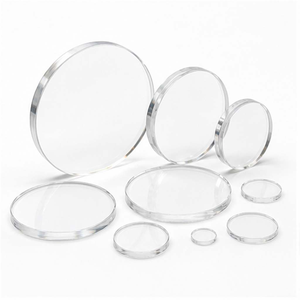
How do you verify optical transmission rates for viewport windows and spectrophotometer discs?
What are your typical prototype and production lead times for Yokohama industrial buyers?
Accelerate Your Semiconductor & Optical Quartz Projects
Send your CAD drawings or technical specifications today. Our engineering desk provides tolerance validation, material grade optimization, and formal quotes within 1 hour.