Engineering White Paper: OEM Semiconductor Quartz Carriers for Monaco's Advanced Microelectronics Industry
The Principality of Monaco, while globally renowned for its financial and luxury sectors, maintains an increasingly sophisticated high-tech manufacturing ecosystem. Specialized cleanroom facilities in the Fontvieille industrial district, coupled with advanced research initiatives supported by Monaco Tech and regional aerospace and oceanographic research institutes, demand world-class component precision. Within semiconductor wafer fabrication, micro-electromechanical systems (MEMS) production, and piezoelectric acoustic sensor manufacturing, custom fused quartz boats and wafer carriers serve as indispensable structural backbone components.
As a global direct-factory manufacturer based in Donghai—China’s premier quartz processing hub—Donghai Kemzo Quartz Products Co., Ltd. provides specialized OEM and ODM engineering services for Monaco-based research labs, micro-OEMs, and semiconductor foundries. This white paper addresses the chemical kinetics, thermomechanical behavior, tolerance constraints, and supply chain considerations required when specifying quartz wafer carriers for high-temperature diffusion, oxidation, and vapor deposition processes.
1. Material Science & Purity Requirements in Wafer Carrier Fabrication
Semiconductor wafer processing environments, specifically high-temperature thermal diffusion ($1000^\circ\text{C} - 1200^\circ\text{C}$) and Low-Pressure Chemical Vapor Deposition (LPCVD), are extraordinarily sensitive to metallic contamination. At elevated thermal regimes, alkali metals such as Sodium ($\text{Na}$), Potassium ($\text{K}$), and Lithium ($\text{Li}$), as well as transition elements like Iron ($\text{Fe}$), Copper ($\text{Cu}$), and Chromium ($\text{Cr}$), can rapidly migrate out of low-grade glass carriers and thermally diffuse directly into silicon or gallium nitride ($\text{GaN}$) crystal lattices. This auto-doping effect results in catastrophic carrier lifetime degradation, gate oxide breakdown, and erratic threshold voltages in processed micro-chips.
| Trace Impurity Element | Standard Commercial Grade (PPM) | Kemzo Semiconductor Grade (PPM) | Impact on Wafer Processing |
|---|---|---|---|
| Aluminum (Al) | 15.0 - 25.0 | < 8.0 | Prevents acceptor-level lattice distortion. |
| Iron (Fe) | 0.8 - 1.5 | < 0.2 | Eliminates deep-level metallic traps in silicon substrates. |
| Sodium (Na) | 1.0 - 2.0 | < 0.3 | Prevents mobile ion contamination in gate dielectrics. |
| Potassium (K) | 0.8 - 1.2 | < 0.2 | Mitigates high-temperature drift instability. |
| Lithium (Li) | 0.5 - 1.0 | < 0.1 | Prevents rapid interstitial diffusion under bias voltage. |
| Hydroxyl Group (OH⁻) | 15.0 - 30.0 | < 5.0 (Low-OH Option) | Suppresses glass softening & thermal devitrification. |
By extracting high-purity natural silica sand from Donghai’s unique geological formations and applying multi-stage chemical acid leaching, magnetic separation, and vacuum flame fusion, Kemzo produces fused quartz structural elements exhibiting total trace element contamination well under 20 PPM, with specialized semiconductor grades reaching 99.99% SiO₂ purity.
2. Mechanical Structural Geometry: Horizontal vs. Vertical Quartz Boats
Semiconductor foundries and micro-fabrication laboratories operating in Monaco utilize two dominant furnace architectures, each demanding custom-engineered boat geometries:
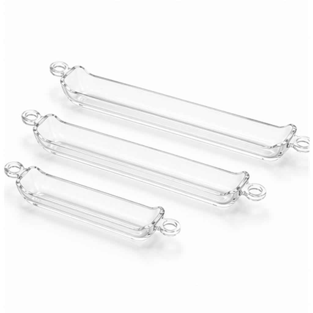
- Horizontal Diffusion & Oxidation Boats: Typically constructed as 4-rod or ladder-style assembly structures. The slots are precision-milled using multi-axis CNC diamond grinding tools to create smooth, stress-free micro-grooves. Fire-polishing the slot radii is vital to eliminate micro-fractures that could act as nucleation sites for thermal shock cracking during rapid furnace insertion and extraction.
- Vertical Batch Furnace Shell Boats: Designed for high-density vertical furnace systems used in LPCVD (Nitride, Polysilicon, and TEOS deposition). These structures consist of precision-perforated quartz plates or solid quartz rods joined via high-temperature plasma welding. Vertical boat assemblies require strict concentricity tolerances (within $\pm 0.05\text{mm}$) to guarantee smooth robotic wafer transfer via Automated Guided Vehicles (AGVs) and cleanroom end-effectors.
3. Thermomechanical Stress & Devitrification Kinetics
Fused quartz possesses an exceptionally low Coefficient of Thermal Expansion (CTE) of approximately $5.5 \times 10^{-7} /^\circ\text{C}$ between $20^\circ\text{C}$ and $300^\circ\text{C}$. This property empowers quartz carrier boats to withstand rapid thermal ramps ($> 15^\circ\text{C}/\text{min}$) without structural warp or thermal-stress-induced fracture. However, when operating continuously above $1150^\circ\text{C}$, fused silica undergoes a phase transformation process known as devitrification, where the amorphous glass structure transitions into crystalline β-cristobalite.
Cristobalite formation begins at surface defect sites or points contaminated with alkali trace elements. Because cristobalite undergoes a significant volume change during cooling around $220^\circ\text{C}$ ($\alpha \leftrightarrow \beta$ inversion), devitrified surface zones experience severe stress, leading to micro-spalling and particulate contamination on process wafers. Kemzo’s proprietary surface-annealing protocols and high-purity flame-polishing processes minimize surface defect density, extending boat operational service life by up to 35% compared to standard commercial quartz carriers.
Micro-Sensor & MEMS Wafer Fabrication
Monaco's specialized micro-engineering labs produce ultra-compact piezoelectric and pressure sensors for luxury marine, aerospace, and medical diagnostic instruments. Our custom slot-pitch horizontal quartz boats ensure uniform gas distribution during critical thin-film deposition cycles.
Cleanroom R&D at Fontvieille Tech Facilities
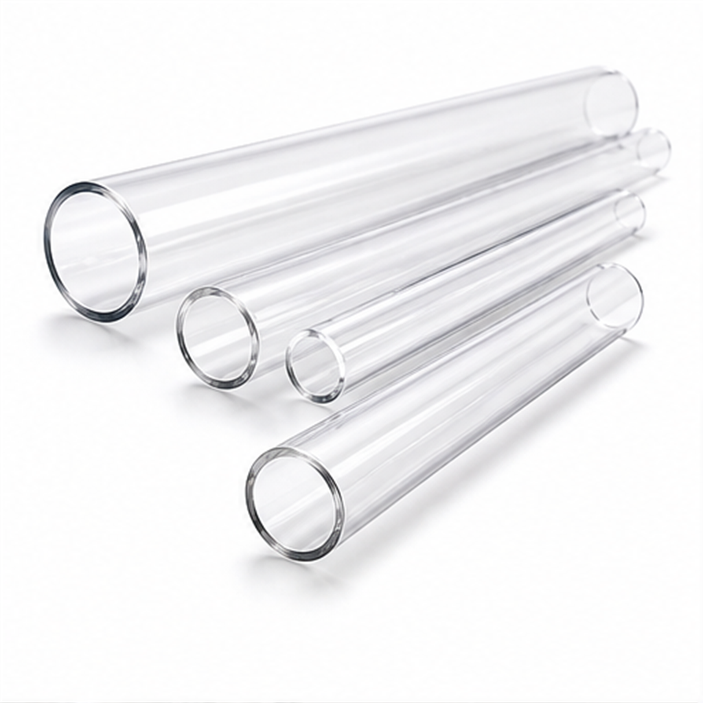
Providing high-purity single-crystal quartz substrates, ground-joint reaction tubes, and analytical combustion vessels to cleanroom research units in Fontvieille, supporting rapid prototyping of next-generation micro-optoelectronic devices.
High-Frequency QCM Biosensor Development
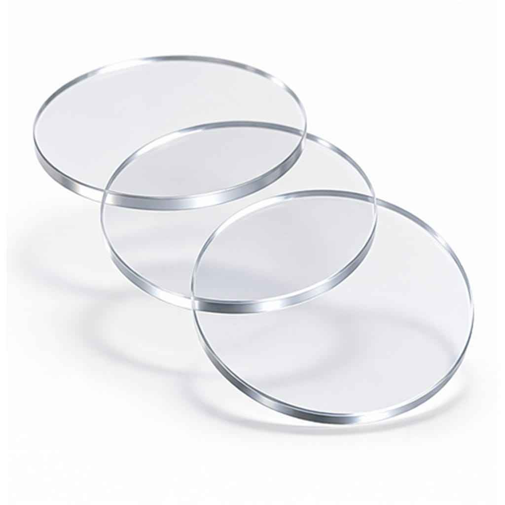
Precision-chamfered optically polished single-crystal quartz wafers supplied to Monaco’s oceanographic and bio-tech research groups for Quartz Crystal Microbalance (QCM) sensors capable of nanogram-level real-time mass detection.
Regional Technology Trends: Smart Micro-Fab & Sustainable Quartz Lifecycle in Western Europe
As the European Union and adjacent tech hubs like Monaco accelerate investment under the European Chips Act framework, regional semiconductor research and specialized fabrication foundries are prioritizing three major operational shifts:
1. Extreme Slot Pitch Tolerances for Automated Handling
Modern cleanrooms in Monaco and Southern France are increasingly adopting robotic wafer loading systems. Manual wafer placement is being replaced by robotic end-effectors requiring slot pitch accuracy down to $\pm 0.02\text{mm}$ and perpendicularity tolerances within $\pm 0.05^\circ$. Kemzo utilizes ultra-precision CNC diamond cutting machinery and laser inspection setups to meet these rigid semi-standard specifications (SEMI E1.9).
2. Closed-Loop High-Purity Silica Recycling
Aligning with Monaco’s strict Environmental Policy and Green Economy Directives, high-tech manufacturing partners are demanding sustainable quartz lifecycles. Kemzo provides specialized re-fabrication and re-polishing services, allowing damaged or devitrified quartz boats to be stripped, fire-polished, annealed, and re-certified for cleanroom reuse, reducing material waste by up to 60%.
3. Low-OH Material Integration for Extended Photolithography & UV Curing
With deep UV (DUV) photolithography and optical curing expanding across European micro-OEMs, quartz components must exhibit high optical transmission down to 193 nm. By controlling hydroxyl ion concentrations to under 5 PPM, Kemzo’s synthetic and high-purity fused silica parts eliminate UV color-center formation and prevent solarization degradation over extended UV exposure runs.
Why Global Procurement Teams Partner with Donghai Kemzo Quartz
Founded in 2011 in Donghai County—China’s world-renowned crystal and silica capital—Donghai Kemzo Quartz Products Co., Ltd. has grown into a premier integrated manufacturer and exporter of high-purity quartz products. Recognized as an official Jiangsu High Technology Enterprise and certified under ISO 9001 Quality Management Systems, Kemzo operates state-of-the-art facilities covering over 3,000 square meters.
Source Cluster Material Access
Direct proximity to Donghai’s raw quartz reserves enables strict raw material selection, maintaining SiO₂ purity up to 99.99% while offering unmatched cost stability.
10+ Production & CNC Lines
Equipped with multi-axis CNC glass grinding mills, precision lathe flame-welding stations, laser slicing machines, and optical polishing lines.
70%+ Annual Export Ratio
Servicing advanced technology buyers across North America, Europe, East Asia, and Oceania with international trade compliance and multi-currency options (USD, EUR, GBP).
1-Hour Technical Feedback
Our dedicated team of glass engineers and international trade specialists provides rapid drawing feasibility reviews and transparent quotes within 1 hour.
Need Custom OEM Quartz Boats Manufactured for Monaco Cleanrooms?
Submit your CAD drawings, wafer carrier dimensions, or process specs today. Receive rapid engineering feedback, material grade recommendations, and direct factory pricing within one hour.