Featured Fused Quartz Products & Substrates
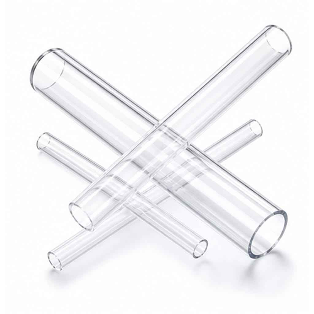
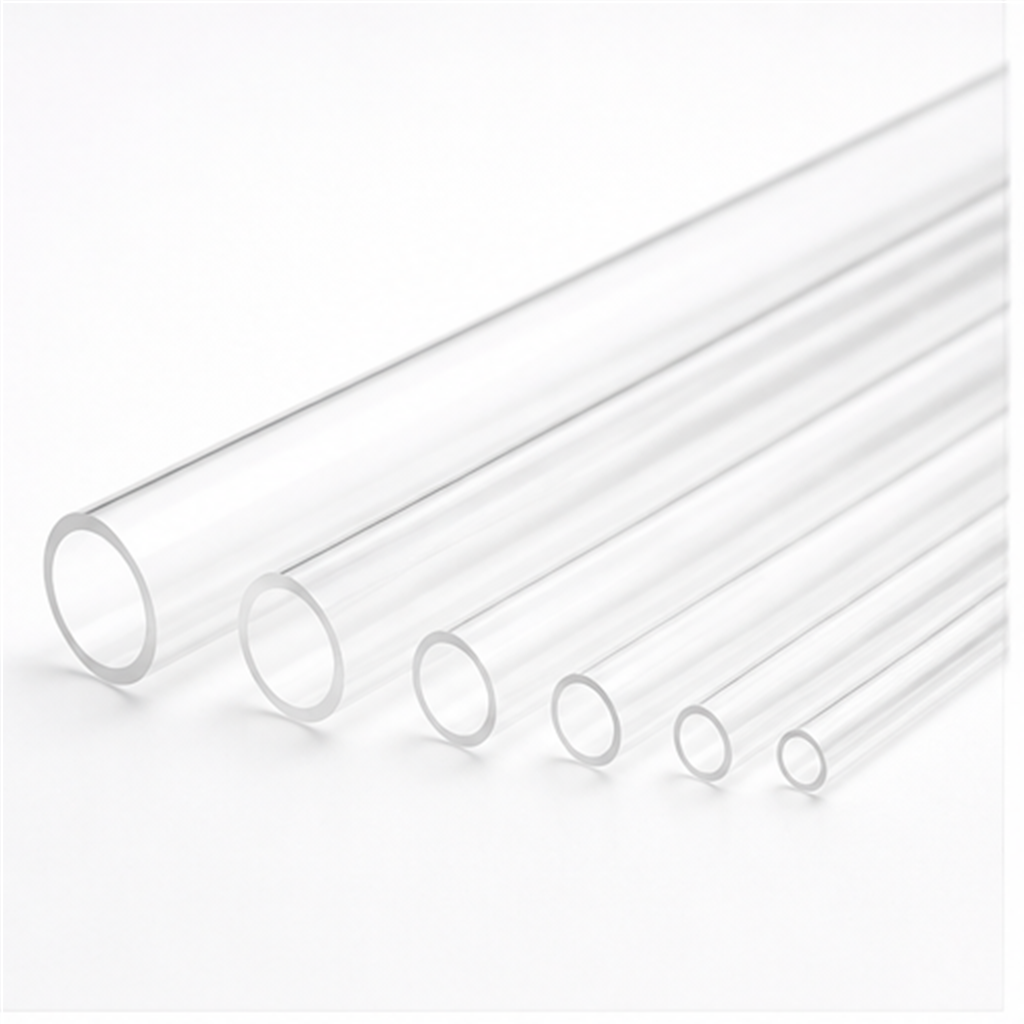
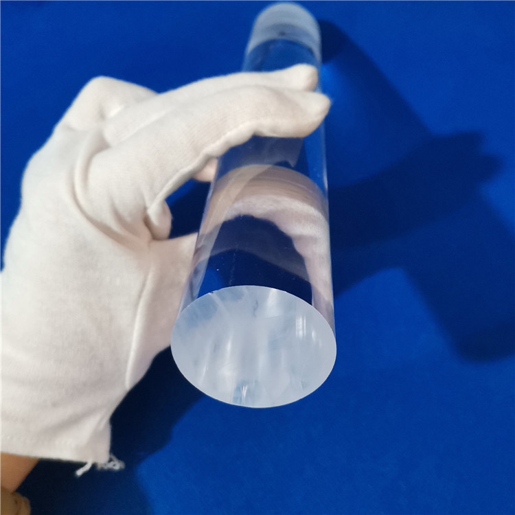
High-purity quartz plates, process tubes, and specialized crucibles fabricated for semiconductor, optical, and industrial high-temperature applications.
Semiconductor Photomask Quartz Plates: Engineering & Optical Physics
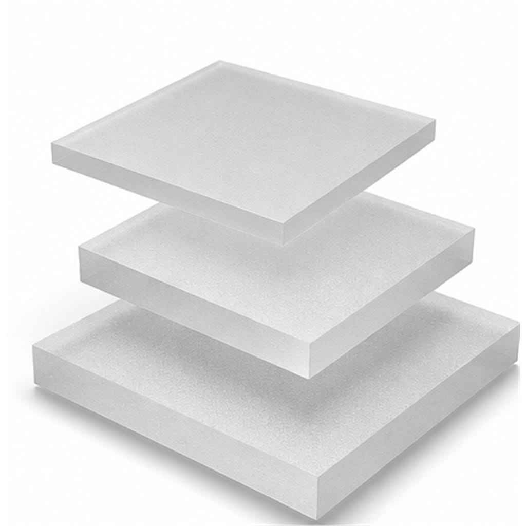
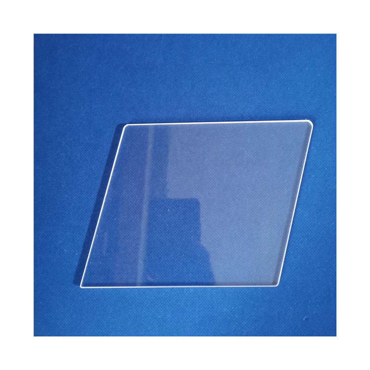
In modern deep-ultraviolet (DUV) and extreme-ultraviolet (EUV) photolithography, the photomask blank substrate serves as the primary master optical element. It transfers intricate, micro- and nano-scale integrated circuit (IC) patterns onto silicon wafers. Donghai Kemzo Quartz Products Co., Ltd. manufactures ultra-high purity synthetic fused silica photomask plates engineered specifically to meet the rigorous thermal, optical, and geometric requirements of leading semiconductor foundries, MEMS producers, and photonics research institutes.
Ultra-Low Coefficient of Thermal Expansion (CTE)
During high-energy laser exposure (such as ArF 193nm or KrF 248nm excimer lasers), intense photonic absorption can induce thermal gradients across the photomask plate. Our synthetic photomask quartz plates exhibit an extremely low CTE of 0.55 × 10⁻⁶ / °C (between 20°C and 320°C). This minimal thermal deformation prevents pattern placement errors, grid distortion, and overlay misalignment during critical step-and-scan lithography cycles.
Deep Ultraviolet (DUV) Transmission Efficiency
Standard borosilicate or low-grade natural fused quartz suffers from metallic impurity absorption (Fe, Ti, Na) and solarization under sub-300nm radiation. Kemzo's high-purity synthetic quartz plates (JSU/JSG grades) feature internal transmittance exceeding 99.5% at 193nm and 248nm, combined with near-zero hydroxyl (OH) content options. This prevents solarization-induced darkening and phase-shift aberration over millions of laser pulses.
Material Information Gain: Synthetic Fused Silica vs. Natural Fused Quartz
While natural fused quartz (melted from high-grade pegmatite quartz crystals) is ideal for diffusion furnace tubes, sight glass, and melting crucibles, semiconductor photomasks demand synthetic fused silica synthesized from vaporized silicon tetrachloride (SiCl4). This chemical synthesis eliminates bubble inclusions down to ISO 10110-3 Class 0/0 standards and reduces total metallic impurities to under 0.1 ppm, ensuring zero optical scattering in sub-micron photolithography.
Substrate Flatness & Surface Polish Specifications
Photomask fabrication requires sub-nanometer surface roughness to ensure atomic-level adhesion of chromium (Cr), molybdenum silicide (MoSi), or anti-reflective coatings (ARC). Kemzo utilizes advanced Chemical Mechanical Planarization (CMP) and double-side optical polishing to achieve standard industry specifications:
| Standard Plate Format | Dimensions (mm) | Thickness (mm) | Flatness (TTV) | Surface Quality (Scratch-Dig) | Primary Application |
|---|---|---|---|---|---|
| 6060 Photomask Blank | 152.4 × 152.4 (6" × 6") | 6.35 mm (0.250") | < 0.5 μm | 10-2 / 10-5 ISO 10110 | Standard IC Lithography / DUV Reticles |
| 7070 Photomask Blank | 177.8 × 177.8 (7" × 7") | 2.28 mm / 3.0 mm | < 0.8 μm | 20-10 Scratch-Dig | Large Format IC & Compound Semi |
| 5050 Photomask Blank | 127.0 × 127.0 (5" × 5") | 2.28 mm / 5.0 mm | < 0.8 μm | 20-10 Scratch-Dig | MEMS, Discrete Devices & Optoelectronics |
| Custom Round/Square | 10.0 mm to 300.0 mm | 0.5 mm to 25.0 mm | Up to λ/10 @ 632.8nm | 10-2 Precision Optical | E-Beam Lithography & Microfluidic Masters |
Localized Application Scenarios in London & the Greater UK Ecosystem
Empowering London’s world-class nanotechnology cleanrooms, quantum computing clusters, and semiconductor research facilities with high-precision quartz substrates.
1. London Academic & University Cleanrooms
London hosts tier-one academic research institutions, including Imperial College London (London Centre for Nanotechnology), University College London (UCL), and King's College London. Our synthetic quartz plates serve as critical photomask blanks for electron-beam lithography (EBL) and direct laser writing in prototyping quantum dot devices, photonic integrated circuits (PICs), and bio-MEMS sensors.
2. Silicon Fen & Golden Triangle Supply Corridor
London forms the anchor of the UK's 'Golden Triangle' research corridor connecting London, Cambridge, and Oxford. Serving tech spinoffs and compound semiconductor startups across Cambridge's Silicon Fen and Thames Valley, Kemzo supplies custom-dimensioned quartz substrate plates optimized for Gallium Nitride (GaN) and Silicon Carbide (SiC) power semiconductor masking processes.
3. Industrial Photonics & Quantum Hardware
As London emerges as a global epicenter for quantum computing software and hardware prototyping (e.g., trapped-ion hardware and quantum key distribution), our ultra-flat optical quartz plates provide the high damage threshold and low birefringence necessary for UV beam splitter windows, reticle carriers, and vacuum chamber viewports.
UK & London Market Trends in Semiconductor Materials
Strategic supply chain alignment with the UK National Semiconductor Strategy and European advanced manufacturing benchmarks.
Surge in UK Sovereign Chip Design & Prototyping
Following the release of the UK Government’s £1 Billion National Semiconductor Strategy, London has experienced an acceleration in fabless chip design houses requiring local pilot-line manufacturing. Because full-scale mask sets from overseas foundries incur high NRE (Non-Recurring Engineering) costs, London labs rely on Kemzo’s fast-turnaround raw blank quartz plates to fabricate in-house master reticles, drastically shortening design-to-wafer verification cycles.
Demand for High Net-Zero & Responsible Sourcing
UK and European tech buyers prioritize carbon transparency, ISO compliance, and sustainable quartz refining. Operating from Donghai, Jiangsu—the premier raw quartz processing hub—Donghai Kemzo Quartz Products Co., Ltd. implements energy-efficient melting and closed-loop water filtration for CMP polishing, matching the stringent ESG and environmental metrics mandated by London corporate buyers and European green standards.
Why London Procurement Managers Choose Kemzo Quartz
Direct factory capabilities from Donghai, China’s quartz capital, delivering uncompromised purity and precision since 2011.
Donghai Source Origin
Located at 7 North Huaya Road, Donghai County, Lianyungang, we leverage direct raw material reserves for ultra-pure natural and synthetic quartz feedstocks.
ISO 9001 Certified Quality
Rigorous quality management covering spectrophotometer UV transmission testing, laser interferometric surface measurement, and zero-defect visual checks.
Complete In-House OEM Machining
Over 11 years OEM/ODM experience providing custom CNC milling, edge beveling, laser scribing, optical polishing, and chrome coating preparations.
Direct Express to London Hubs
Exporting over 70% of output worldwide. Specialized shockproof packaging ensures safe door-to-door delivery via DHL/FedEx air freight directly into London.
Fused Quartz Material Grade Selection Guide
Select the optimal material specification based on thermal, optical, and mechanical performance requirements.
| Quartz Material Grade | SiO2 Purity (%) | OH Content (ppm) | UV Cut-off Wavelength | Max Operating Temp | Typical Applications |
|---|---|---|---|---|---|
| Synthetic Fused Silica (JSU-1 / Corning 7980) | ≥ 99.999% | < 5 ppm (Low OH) / ~1000 ppm | 160 nm (Deep UV) | 1100 °C (Continuous) | ArF (193nm) & KrF (248nm) Photomask Plates, UV Laser Windows |
| Optical Grade Fused Quartz (JSU-2) | ≥ 99.99% | < 30 ppm | 220 nm | 1150 °C | Microscope Slides, Sight Glass, UV Spectroscopy Cuvettes |
| Clear Process Fused Quartz (Kemzo Tube Grade) | ≥ 99.9% | < 15 ppm | 260 nm | 1200 °C (Short term 1450 °C) | Diffusion Furnace Tubes, Vacuum CVD Process Chambers, Chemical Piping |
| Opaque / Milky Quartz Glass | ≥ 99.9% | N/A (Micro-porous structure) | Opaque (Infrared Diffuse) | 1250 °C | Melting Crucibles, Heat Shields, Thermal Flanges & Insulation Ring |
Frequently Asked Questions (FAQ) for London & Global Procurement
Clear technical and commercial answers to streamline your quartz substrate purchasing process.
How do synthetic fused silica photomask plates differ from standard quartz plates?
Synthetic fused silica is chemically synthesized from silicon-containing gases (such as SiCl4) in an oxygen-hydrogen flame, resulting in zero bubble inclusions (ISO 10110-3 class 0/0) and total metallic impurities under 0.1 ppm. Standard quartz plates are melted from natural quartz crystals, which contain trace metallic impurities (Fe, Al, Ti) that absorb deep ultraviolet (DUV) light. For lithography mask applications below 300nm, synthetic fused silica is essential to prevent laser damage and distortion.
What tolerances and surface finishes can Kemzo achieve for custom photomask plates?
Kemzo can achieve dimensional tolerances down to ±0.05 mm, thickness tolerances within ±0.02 mm, and Total Thickness Variation (TTV) under 0.5 μm. Our optical polishing capabilities yield surface roughness (Ra) below 0.2 nm (2 Angstroms) and surface quality up to 10-2 Scratch-Dig according to MIL-PRF-13830B or ISO 10110 standards.
What is the typical shipping lead time to London and the United Kingdom?
For standard dimensioned raw blanks or stock sizes, orders dispatch within 3 to 5 working days. Custom CNC machined, chamfered, and CMP polished photomask plates generally require 10 to 15 business days for fabrication. Express air freight via FedEx, DHL, or UPS reaches London Heathrow (LHR) or London Stansted (STN) within 3 to 5 transit days.
Can you provide custom chamfering, alignment notches, and chrome coating prep?
Yes. We offer complete custom edge profiling, including 45-degree beveling, safety edge grinding, SEMI-standard orientation notches, laser engraved serial markers, and specialized ultrasonic cleanroom washing (Class 100) ready for sputtering chromium (Cr) or MoSi thin films.
How do you ensure fragile quartz glass plates arrive undamaged during international transit?
Every photomask plate is enclosed in individual cleanroom-safe dust-free gel boxes or vacuum-sealed anti-static pouches, isolated by shock-absorbing PE foam sleeves, and packed into reinforced export-grade wooden crates. We maintain an export damage rate of virtually zero across thousands of shipments to Europe and North America.
What quality documentation and material test reports (MTR) are provided?
With every export lot, we provide a Certificate of Analysis (COA) detailing chemical purity (GDMS analysis), UV transmission curves (193nm / 248nm / 365nm spectral sweep), surface roughness interferometry reports, and dimensional inspection sheets.
Need High-Precision Photomask Quartz Substrates in London?
Send your engineering drawings (CAD / STEP / PDF) or technical specs to Donghai Kemzo Quartz Products Co., Ltd. Our engineering specialists will provide a detailed quote and material feasibility review within 1 hour.