≥ 99.999%
Synthetic Silica Purity
Ra ≤ 0.2 nm
Atomic Scale Smoothness
≤ 0.5 ppm/K
Thermal Expansion (CTE)
ISO 9001
Certified Foundry Operations
Lithography & Microfabrication Portfolio
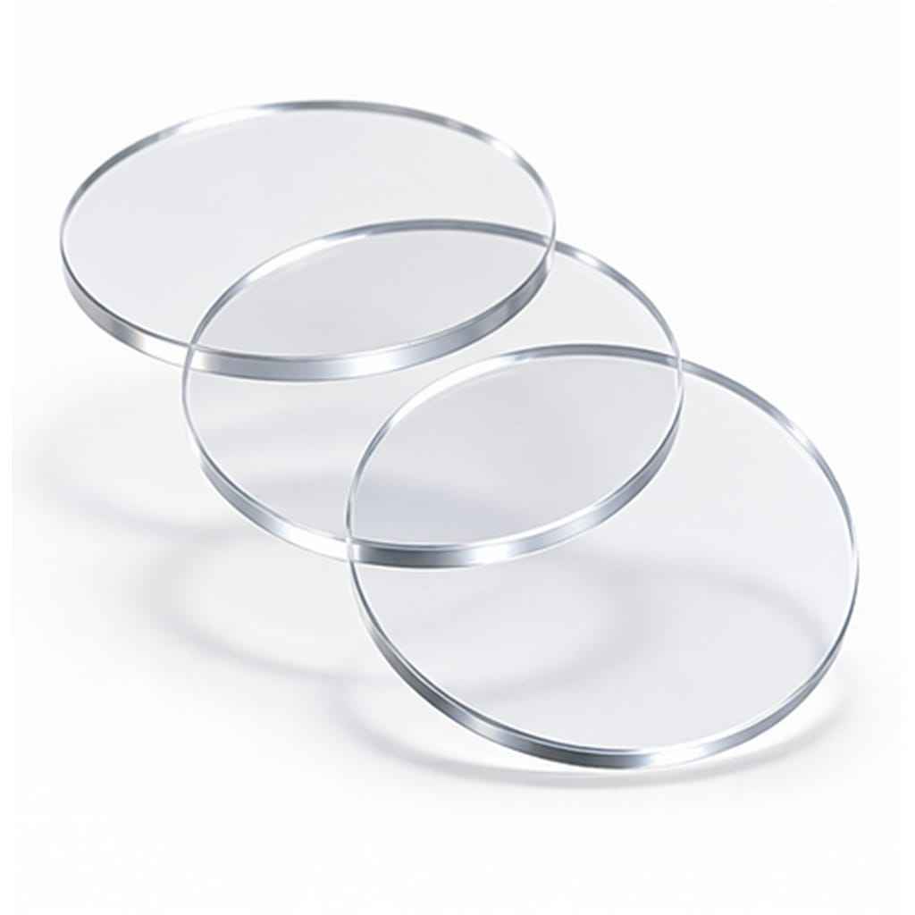
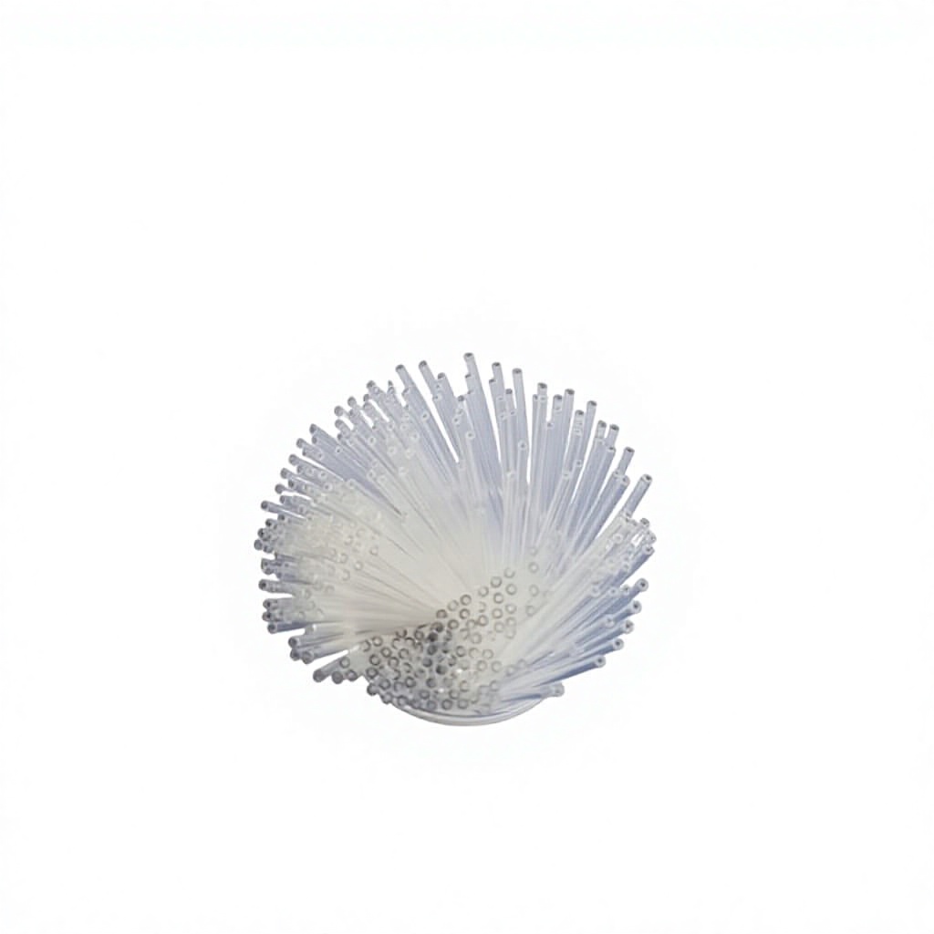
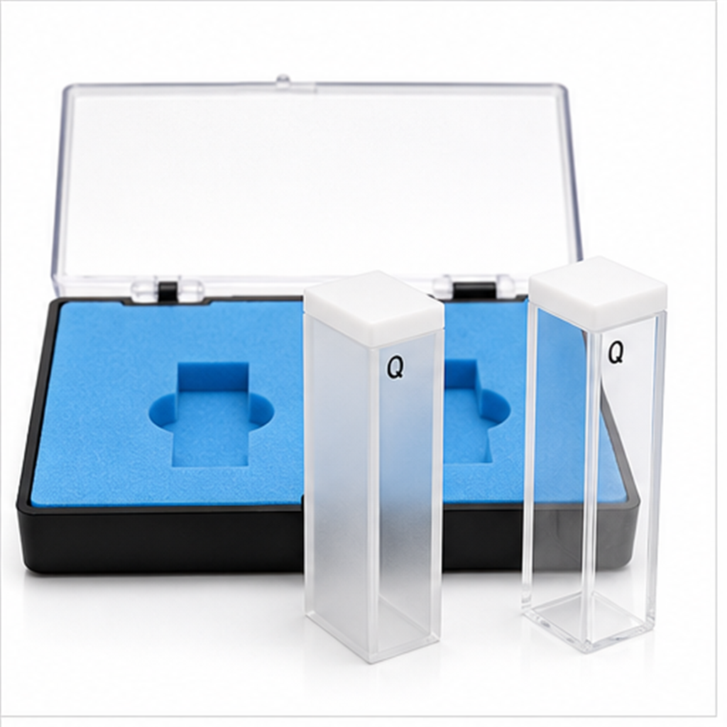
Precision Semiconductor Quartz Substrates & Optical Ware
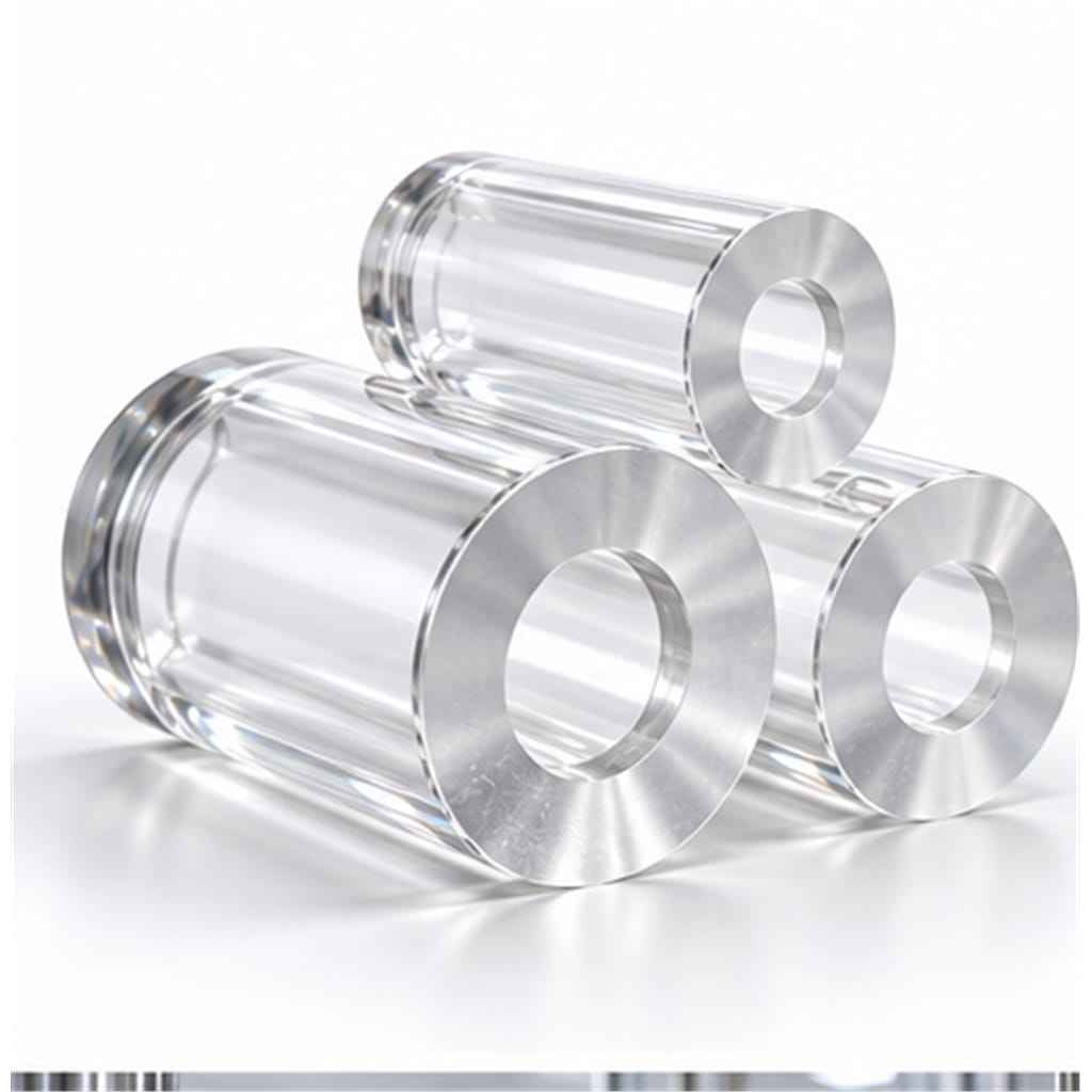
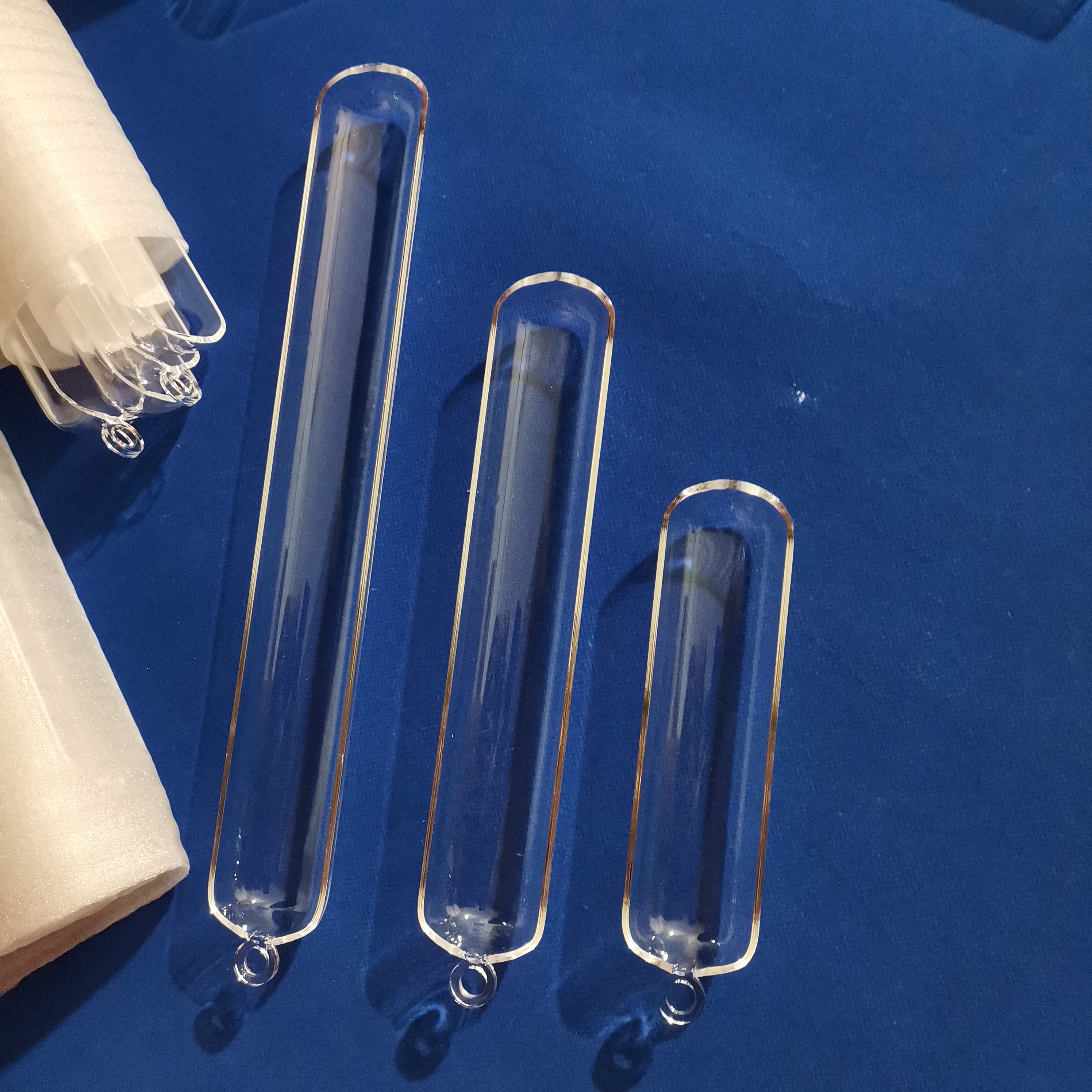
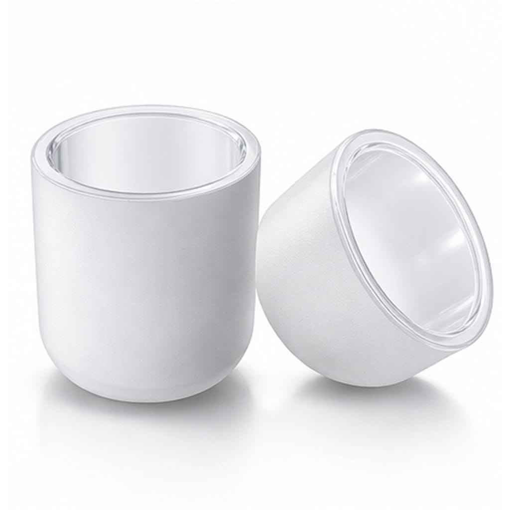
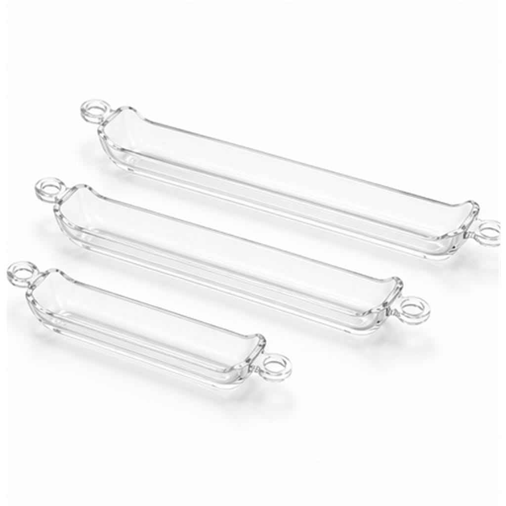
Direct from our Donghai facility: specialized fused silica blanks, double-side polished plates, combustion vessels, and wafer handling systems delivered with certified flatness and traceability to Parisian research labs and industrial foundries.
Technical White Paper
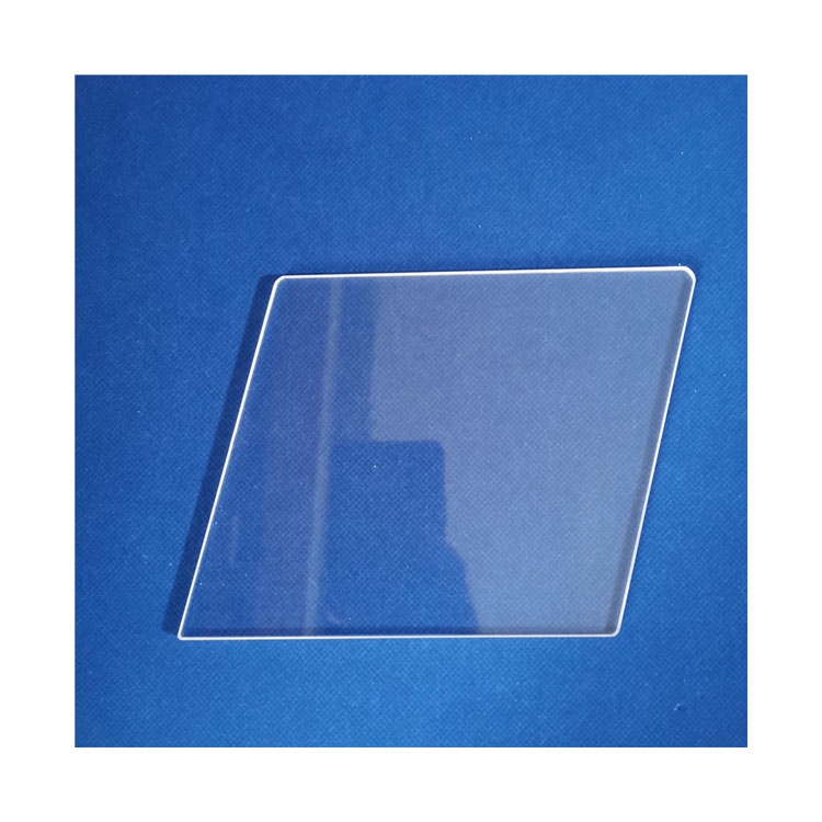
Semiconductor Photomask Quartz Plate Engineering: Metrology, Defectivity, and DUV Transmittance
A rigorous examination of substrate stability, synthetic chemical vapor deposition (CVD) silica synthesis, and the physical parameters governing sub-micron photolithography transfer integrity.
In modern microlithography and nano-pattern replication, the photomask blank serves as the master blueprint from which billions of microelectronic circuits are etched onto silicon wafers. Any volumetric inhomogeneity, metallic inclusion, surface stria, or thermal deformation within the underlying quartz substrate directly compromises pattern fidelity, introducing critical dimension (CD) variations, phase aberrations, and unacceptable run-out errors. As integrated device manufacturers (IDMs), pure-play MEMS foundries, and advanced optoelectronic institutes in Paris and the broader Île-de-France region scale down to deep-submicron features, standard optical soda-lime or borosilicate glasses become entirely unusable due to significant thermal expansion and prohibitive deep-ultraviolet (DUV) attenuation.
Donghai Kemzo Quartz Products Co., Ltd. addresses these microfabrication bottlenecks by manufacturing ultra-high-purity synthetic fused silica (a-SiO₂) photomask quartz plates. Utilizing high-temperature hydrolysis of high-purity silicon tetrachloride (SiCl₄), our synthesis produces synthetic amorphous silica practically free from refractory heavy metals and bubble inclusions. Below 250 nm, our photomask blanks exhibit exceptional internal transmittance (≥ 90.5% at 193 nm ArF and ≥ 92.0% at 248 nm KrF excimer lines), while preserving an ultra-low coefficient of thermal expansion of approximately 5.5 × 10⁻⁷/°C across ambient to intermediate process temperatures.
"The mechanical stability of a lithography reticle depends strictly on residual stress birefringence and surface profile flatness. Our double-side chemical-mechanical planarization (CMP) workflow routinely achieves Total Thickness Variation (TTV) below 1.0 μm across a 6025 (6 × 6 × 0.25 inch) format, eliminating focal plane tilt during high-numerical-aperture exposure runs."
Critical Material Properties for Semiconductor Photomask Blanks
A photomask blank is not simply an optical filter; it is a structural element exposed to intensive pulsed laser irradiation, dry etching plasma chemistries, and repetitive SC-1/piranha wet chemical cleans. The physical and chemical specifications below represent our standard foundry baselines for semiconductor-grade photomask plates exported to European nanofabrication centers.
| Physical / Optical Parameter | Synthetic Fused Silica (Litho-Grade) | Purified Natural Fused Quartz | Lithographic Significance |
|---|---|---|---|
| Purity (Total Metallic Contaminants) | < 0.1 – 0.5 ppm wt (Fe, Cu, Ni, Cr < 5 ppb) | < 10 – 20 ppm wt | Prevents photo-induced center darkening & metal contamination |
| Transmittance @ 193 nm (ArF, 6.35 mm) | ≥ 90.5% (Internal ≥ 99.5%/cm) | < 20% (Severe band-gap cutoff) | Enables sub-45nm feature exposure with minimal pulse attenuation |
| Transmittance @ 248 nm (KrF, 6.35 mm) | ≥ 92.0% | ≥ 88.0% | Optimal for standard UV/DUV mask projection lithography |
| Total Thickness Variation (TTV) | ≤ 1.0 μm (Custom ≤ 0.5 μm) | ≤ 2.5 μm | Guarantees focal depth uniformity across 152 × 152 mm field |
| Surface Roughness (Atomic Ra) | ≤ 0.15 – 0.25 nm (AFM measurement) | ≤ 0.5 nm | Eliminates light scatter and ensures pinhole-free Cr/MoSi adhesion |
| Internal Stress Birefringence | ≤ 1.0 nm/cm (Polarimeter verified) | ≤ 5.0 nm/cm | Maintains beam polarization integrity without wavefront phase shift |
| Thermal Expansion Coeff. (0–200 °C) | 0.52 × 10⁻⁷ /°C | 0.55 × 10⁻⁷ /°C | Prevents run-out and registration errors under intense illumination |
Regional Ecosystem Integration
Localized Applications Across the Greater Paris & French Deep-Tech Ecosystem
From university cleanroom consortiums in Palaiseau to silicon photonics spin-offs along the Seine corridor, our quartz plates provide the structural and optical foundation for mission-critical micro-engineering.
Paris-Saclay Nanotechnology Cluster
Supplying standard 5009, 6012, and 6025 double-side polished synthetic silica photomask blanks to research laboratories (including C2N, CNRS, and university cleanrooms) for e-beam lithography, lift-off processing, and advanced compound semiconductor prototyping.
Silicon Photonics & Quantum Foundries
Providing custom chamfered quartz wafers, high-homogeneity windows, and optical plates with sub-angstrom surface finishes, tailored for telecommunication waveguiding circuits, Parisian quantum processor startups, and integrated optics packaging.
Microfluidics & Bio-MEMS in Paris Biotech
Delivering biocompatible, optically transparent fused silica plates for microfluidic chip fabrication, QCM sensor assemblies, and UV-transparent diagnostics, serving medical research centers across the Villejuif and Évry bio-clusters.
Industrial Dynamics in Île-de-France Microelectronics
The semiconductor ecosystem in France is undergoing a strategic resurgence under the European Chips Act and the "France 2030" investment directive. While major commercial volume silicon fabs operate in the Crolles and Grenoble corridors, Paris and the Île-de-France region represent the nation’s premier epicentre for semiconductor research, advanced packaging, optical telecommunications, and defense microelectronics.
Facilities across the Paris-Saclay innovation belt, Corbeil-Essonnes, and specialized cleanroom incubators require reliable, high-mix low-to-medium volume (HMLV) supplies of semiconductor-grade quartzware. Whether for specialized pilot production runs, repair reticles, or custom optical alignment targets, Parisian cleanroom engineers demand materials compliant with REACH and RoHS standards, accompanied by detailed interferometric flatness and surface roughness inspection sheets.
Industry Projections
Emerging Lithography Trends Shaping the French Semiconductor Landscape
Strategic technological evolutions dictate higher tolerance strictness and localized material readiness throughout European microelectronics supply channels.
Transition Toward DUV and Direct-Write Tooling
Increasing reliance on 193 nm and high-density laser direct-write systems demands photomask blanks with absolute transmission uniformity, zero hydroxyl (OH) bubble clusters, and high laser damage threshold (LDT) ratings exceeding 10 J/cm².
Heterogeneous Integration & Glass Interposers
Advanced packaging groups in Paris are evaluating ultra-flat, high-purity quartz plates as intermediate substrates and interposers, capitalizing on fused silica's exceptional dielectric performance, low loss tangent, and matched thermal expansion coefficients.
Resilient Supply Chains & Dual Sourcing
European fab procurement managers actively de-risk single-source dependencies by establishing qualified relationships with specialized foundries capable of delivering drawing-compliant quartz parts, direct OEM replacement tubes, and mask blanks reliably under Incoterms like DAP and DDU Paris.
Manufacturing Excellence
Why Parisian Cleanrooms Rely on Kemzo Quartz Engineering
Combining the mineral heritage of Donghai with state-of-the-art cold processing, CNC ultrasonic machining, and stringent international export management.
Donghai Industrial Heritage
Headquartered in Lianyungang, Jiangsu—the premier crystal and silica hub—Donghai Kemzo leverages raw material selectivity and mature specialized thermal processing infrastructure since 2011.
ISO 9001 Certified Quality
Recognized as a Jiangsu High Technology Enterprise, our end-to-end quality system enforces strict lot-to-lot traceability, 100% optical inspection, and certified compliance with European cleanroom standards.
Precision OEM / ODM Processing
Over 11 years of custom manufacturing experience. We cut, double-side grind, bevel, flame-polish, and ultrasonic-drill custom apertures strictly according to technical customer CAD drawings.
Rapid Technical Feedback (≤ 1 Hour)
Our dedicated engineering export desk guarantees feasibility checks, tolerance validations, and transparent quoting within one hour for international inquiries.
Global Logistics & Incoterms Flexibility
Over 70% export share serving Europe and North America. Full support for FOB, CIF, CFR, EXW, DDU, and express door-to-door delivery with multi-currency handling (EUR, USD).
Class-100 Clean Packaging
Photomask plates and optical flats are sealed in anti-static, particulate-free fluoropolymer cases, foam cushioned, and shipped in export-grade reinforced crating to ensure zero in-transit damage.
Procurement Knowledge Base
Frequently Asked Questions for Sourcing Photomask Quartz Plates in France
Essential guidance for purchasing agents, cleanroom managers, and optical engineers importing high-purity quartz products to Paris.
What are the standard dimensions and thickness tolerances for photomask quartz plates?
Our standard industry configurations correspond directly to international SEMI specifications, including 4009 (4 × 4 × 0.090 inch), 5009 (5 × 5 × 0.090 inch), 6012 (6 × 6 × 0.120 inch), and 6025 (6 × 6 × 0.250 inch / 152 × 152 × 6.35 mm). Thickness tolerances are typically held within ± 0.05 mm, with wedge and parallelism controlled to within 5 arcseconds upon request. Custom rectangular, circular, or drilled profiles are fully accommodated via our high-precision CNC machinery.
How do you distinguish synthetic fused silica from natural fused quartz for photomask use?
Natural fused quartz is manufactured by melting high-purity natural silica sand; while thermally robust and cost-effective, it contains trace metallic impurities (Al, Fe, Ti) that cause strong absorption bands in the DUV spectrum below 260 nm. Synthetic fused silica is chemical-vapor synthesized from silicon tetrachloride precursors, yielding nearly zero metallic impurities (< 0.1 ppm) and an absence of bubble defects, making it strictly mandatory for 193 nm (ArF) and 248 nm (KrF) projection lithography.
What surface roughness (Ra) and flatness (TTV) specifications do you guarantee?
Through double-side Chemical Mechanical Polishing (CMP) utilizing nano-scale ceria and colloidal silica slurries, we achieve an atomic surface roughness Ra ≤ 0.2 nm (verified by Atomic Force Microscopy). For flatness, our semiconductor-grade plates guarantee Total Thickness Variation (TTV) ≤ 1.0 μm, with premium-grade substrates achieving ≤ 0.5 μm across the central 90% quality area, measured via He-Ne laser interferometry.
What are the lead times and shipping logistics for deliveries to Paris and Île-de-France?
Standard inventory blanks ship within 48 to 72 hours. Custom CNC machined, beveled, or custom-dimensioned polished plates generally require 2 to 3 weeks for fabrication and complete interferometric QA testing. We utilize direct air freight into Paris Charles de Gaulle (CDG) or Orly via DHL, FedEx, or air cargo, with typical transit times of 3 to 5 business days, fully supporting DDP, DDU, and CIF delivery terms.
How does Kemzo Quartz package photomask plates to prevent cleanroom contamination and breakage?
Every plate undergoes automated ultrasonic cleaning and is packaged inside high-purity, dust-free polypropylene mask compacts or single-wafer carriers inside a Class-100 clean packaging environment. The individual carriers are vacuum-sealed in static-shielding barrier bags and nested in custom shock-absorbing foam inserts within heavy-wall export wooden cases, preventing mechanical shock, electrostatic discharge (ESD), and surface particulate contamination.
Can you supply chromium-coated (Cr) or phase-shifting (MoSi) blanks?
Kemzo Quartz specializes primarily in bare, ultra-polished fused silica and quartz glass substrates. However, through strategic partnerships with specialized sputtering facilities, we can supply pre-coated blanks featuring standard anti-reflective opaque chromium (Cr/CrOx) and photoresist layers (such as IP3500 or AZ5214) configured to your facility's exact spin-coating specifications.
Connect Directly with Our Quartz Engineering Team
Send your CAD drawings, dimensional requirements, or target surface specifications. Receive a comprehensive feasibility assessment, material certificate overview, and commercial proposal within 60 minutes.
Send an Inquiry