Optical Grade
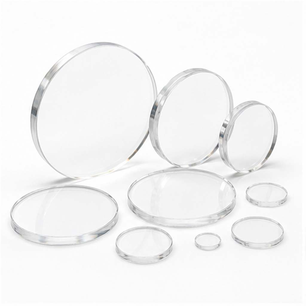
Every substrate and component undergoes laser interferometric calibration, optical surface polishing, and thermal stress relief to meet the stringent zero-defect criteria of microelectronics.
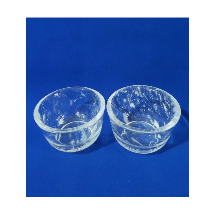
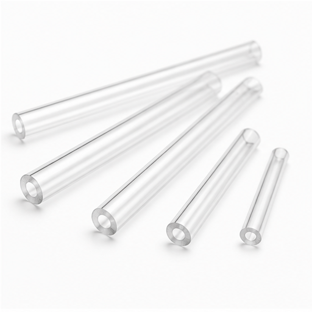
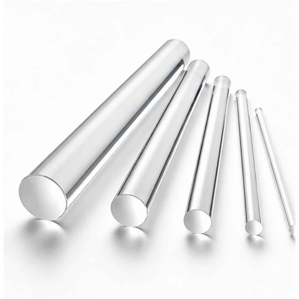
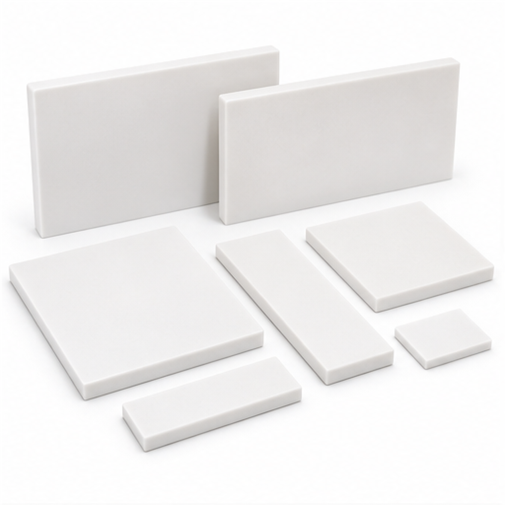
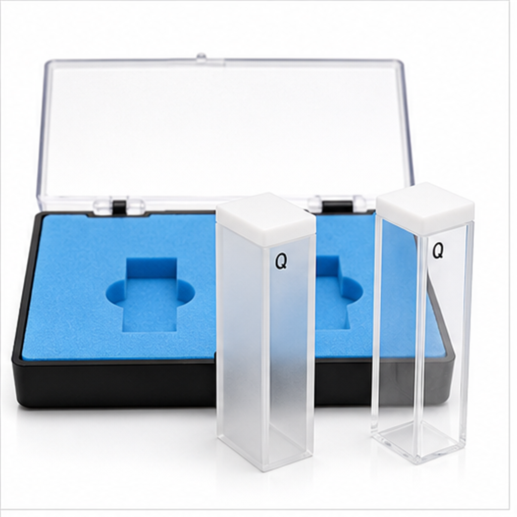
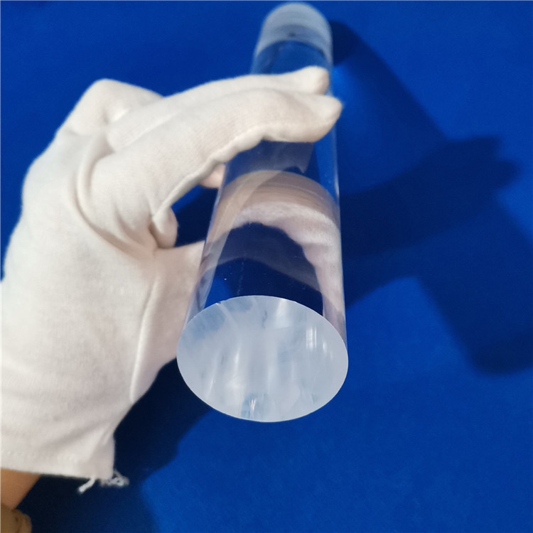
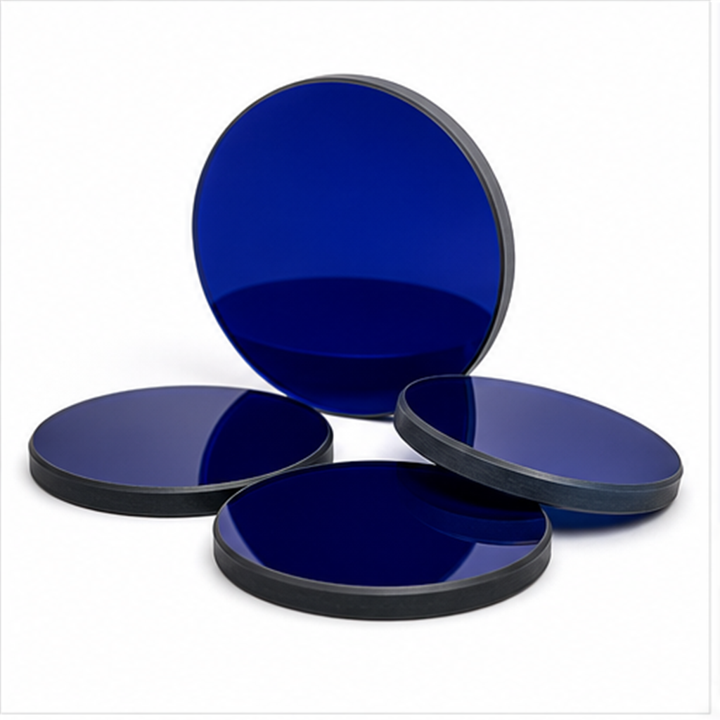
In modern microlithography, the photomask substrate serves as the dimensional anchor for microcircuit patterns. Our synthetic fused silica and electronic-grade quartz plates eliminate thermal wavefront distortions and phase dispersion.
Thermal stability is governed by an ultra-low thermal expansion coefficient of 5.5 × 10⁻⁷ /°C (20°C to 320°C). Under continuous high-fluence DUV (Deep Ultraviolet) exposure, our substrates display zero dimensional shift, preventing mask run-out errors across dense silicon real estate.
Synthesized via chemical vapor deposition of high-purity silicon tetrachloride (SiCl₄), our mask plates achieve internal transmittance surpassing 90.5% at 193 nm (ArF excimer) and over 99.8% at 365 nm (i-line), completely suppressing solarization and optical darkening.
Processed through double-sided planetary polishing and chemical-mechanical planarization (CMP), total thickness variation (TTV) is contained within < 1.5 μm across standard 6-inch plates, with surface roughness (Ra) maintained at ≤ 0.5 nm to guarantee uniform photoresist exposure.
| Physical / Optical Parameter | Semiconductor Photomask Grade | Standard Optical Window Quartz | Engineering Relevance to Buyers |
|---|---|---|---|
| SiO₂ Purity Level | ≥ 99.999% (Synthetic Fused Silica) | ≥ 99.99% (Melted Natural Quartz) | Prevents metallic ion (Fe, Cu, alkali) migration during etching. |
| Bubble & Inclusion Class | Class 0 (Zero bubble in 100 mm aperture) | Class 1 - Class 2 | Eliminates optical projection artifacts and pattern printing defects. |
| Total Thickness Variation (TTV) | ≤ 1.0 μm – 1.5 μm | ≤ 10 μm – 20 μm | Critical for depth-of-focus retention across high-NA projection optics. |
| Refractive Index Homogeneity (Δn) | ≤ 1 × 10⁻⁶ | ≤ 1 × 10⁻⁵ | Ensures identical phase fronts across multi-aperture mask layouts. |
| Thermal Shock Resistance | 1100°C to 20°C Quench without rupture | 1100°C to 20°C Quench without rupture | Immune to thermal cracking under high-power laser writing and baking. |
As Central America deepens its nearshoring capabilities, Guatemala is positioning itself as a technical focal point for micro-optics, specialized MEMS engineering, and sensor component assemblies.
Academic institutions including Universidad de San Carlos de Guatemala (USAC) and Universidad del Valle de Guatemala (UVG) require precision quartz photomask blanks for microfluidics, MEMS prototyping, and nanotechnology microfabrication projects funded by international STEM alliances.
Export manufacturing zones along the Pacific trade corridor and near Mixco utilize high-precision chrome-on-quartz mask blanks for photo-etching micro-sensors, diagnostic biosensor chips, and optical apertures used in surgical instrumentation exported under international medical device accreditations.
Technological facilities supporting the national electrical grid and renewable installations use quartz plates for high-voltage UV arc containment, collimator mask sets, and photodiode arrays, requiring material impervious to volcanic dust, humidity, and tropical ambient stress.
Analyzing supply chain diversification, bilateral trade initiatives, and the long-term regional demand for high-purity quartz substrates across the CAFTA-DR zone.
Guatemala's "Guatemala No Se Detiene" economic policy targets high-value electronics and semiconductors. As North American Tier-1 manufacturers seek assembly, packaging, and testing (ATP) hubs close to the U.S. mainland, local access to precision quartz mask plates has transformed into a critical raw material benchmark.
Historical reliance on standard float or borosilicate glass mask blanks in Central American technical institutes is rapidly ending. The transition toward sub-micron lithography mandates quartz due to its virtually flat thermal curve, ensuring zero image registration drift across variable climate profiles.
Procuring raw quartz products from Donghai—the global epicenter of fused silica melting—enables Guatemalan procurement officers to bypass secondary US/EU reseller markups, securing factory-direct pricing, custom edge chamfering, and guaranteed batch-to-batch chemical homogeneity.
Combining source-origin raw material dominance from China's crystal capital with international ISO 9001 process discipline and seamless logistics to Puerto Quetzal and Santo Tomás de Castilla.
Based in Donghai, Lianyungang, we directly access China's premier high-purity natural silica formations, enabling precise raw sand screening prior to electric arc and hydrogen-oxygen fusion stages.
Over 11 years of custom machining experience. We process CAD/DXF drawings for notched corners, beveled edges, drilled blind holes, stepped profiles, and specialized chromium coating deposition windows.
Every photomask substrate is inspected under monochromatic sodium vapor lighting for internal striations, followed by Zygo laser interferometry for flatness validation before entering cleanroom packaging.
Individual vacuum dust-free carrier encapsulation, anti-static sealed liners, high-density polyethylene suspension foam, and reinforced plywood crates engineered to withstand international transshipment.
Practical answers regarding shipping logistics, material compliance, surface tolerances, and transaction terms for commercial buyers in Central America.
Send us your dimensional drawings, required optical transmission band, or substrate specifications. Our application engineers provide comprehensive quotes, tolerance reviews, and material recommendations within one hour.