Precision Photolithography & Semiconductor Quartz Products
Certified ISO 9001 precision-crafted fused quartz components, synthetic silica substrates, and extreme-environment process vessels tailored for advanced photolithography fabrication facilities and experimental cleanrooms.
White Paper: Semiconductor Photomask Quartz Plate Application in Athens
An engineering overview of photolithography substrate performance criteria, optical transmission profiles, and thermal stability in the evolving Mediterranean semiconductor cluster.
Deep-UV Transparency & Optical Homogeneity
In modern microlithography and nanoimprint lithography (NIL), transmission efficiency below 250 nm (including 193 nm ArF and 248 nm KrF excimer lines) determines edge sharpness and yield. Our synthetic fused silica photomask blanks eliminate internal bubble inclusions and striae, achieving internal transmission exceedances of 99.8% with zero solarization defects under continuous UV exposure.
Near-Zero Thermal Runaway & CTE Stability
Photomask pattern run-out is primarily caused by mask heating during continuous exposure cycles. Standard borosilicate expands significantly under heat load, shifting pattern overlays. Fused quartz features an exceptionally low coefficient of thermal expansion (5.5 × 10⁻⁷ /°C). This allows high-throughput stepper runs at cleanrooms in Athens without dimensional drift or alignment degradation.
Sub-Nanometer Roughness & TTV Control
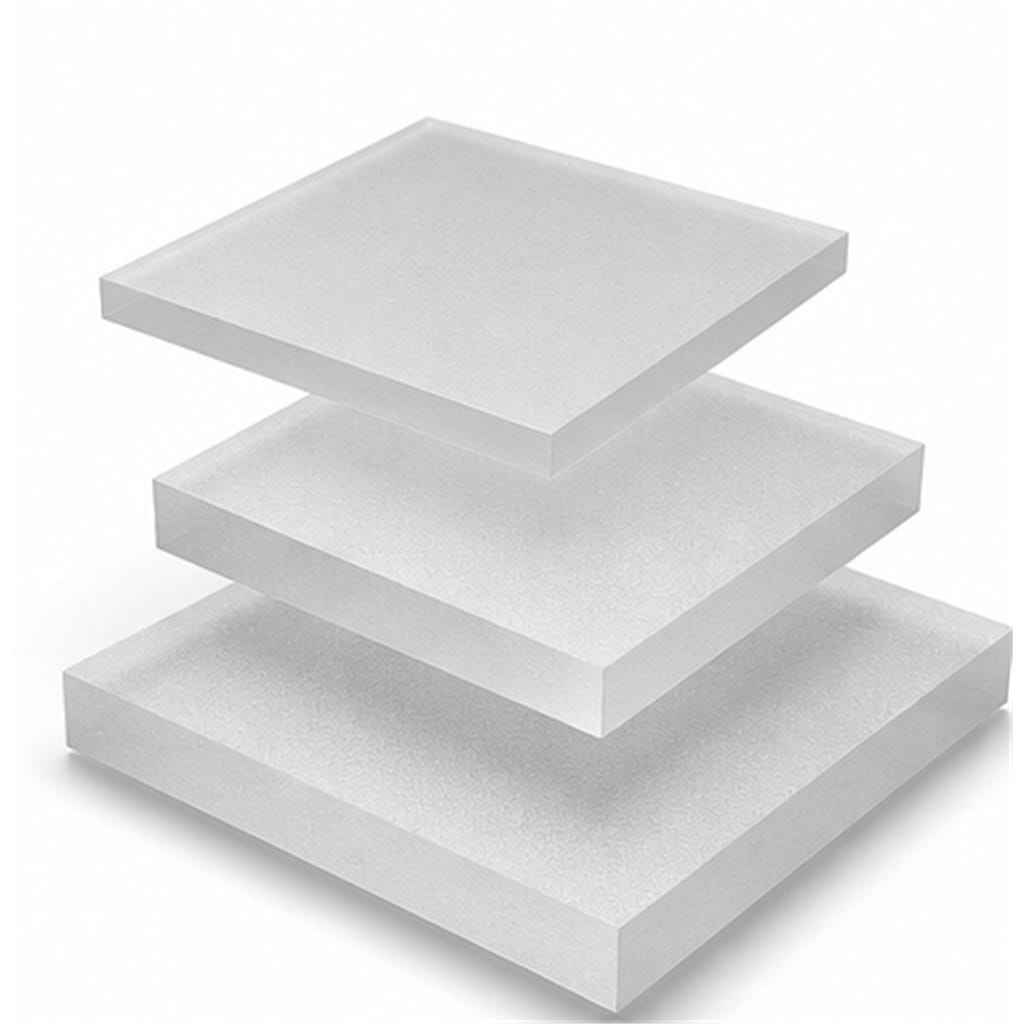
Surface roughness and Total Thickness Variation (TTV) are critical for chromium and phase-shifting film deposition. Our double-sided chemical mechanical planarization (CMP) produces an average roughness (Ra) < 0.3 nm and Total Thickness Variation < 1.5 µm across a standard 6025 (6" × 6" × 0.25") substrate format, preventing pinhole creation during Cr sputtering.
Engineering Material Specifications: Photomask Grade Fused Quartz vs. Borosilicate
Direct comparison of critical photolithographic and thermomechanical metrics validating why high-purity quartz substrates are non-negotiable for semiconductor fabrication.
| Physical & Optical Property | Synthetic Fused Silica (Photomask Grade) | Optical Clear Fused Quartz | Standard Borosilicate (Float) |
|---|---|---|---|
| Purity (SiO₂ Concentration) | > 99.999% | > 99.99% | ~ 80.5% (with alkali metals) |
| Coefficient of Thermal Expansion (20–300°C) | 5.2 × 10⁻⁷ /°C | 5.5 × 10⁻⁷ /°C | 32.5 × 10⁻⁷ /°C (6x higher) |
| Transmission at 193 nm (10 mm path) | > 90.5% | > 80.0% | 0% (Opaque in deep UV) |
| Transmission at 248 nm (10 mm path) | > 92.0% | > 91.0% | < 15% (Severe solarization) |
| Surface Roughness (Ra after CMP) | < 0.25 nm | < 0.40 nm | ~ 1.2 nm |
| Softening Point (°C) | 1683 °C | 1665 °C | 820 °C |
| Dielectric Constant (1 MHz at 25°C) | 3.75 | 3.78 | 4.60 |
Localized Industrial Dynamics & Emerging Applications Across Attica
Exploring how Athens is accelerating from legacy academic research into an active node for photonics packaging, European semiconductor sovereignty, and aerospace sensors.
Attica R&D Centers & NCSR Demokritos Cleanrooms
Athens hosts premier nanotechnology research hubs, notably the Institute of Nanoscience and Nanotechnology (INN) at NCSR Demokritos and the National Technical University of Athens (NTUA). These institutions demand specialized custom quartz plates, wafer lapping carriers, and cleanroom-compatible quartz masks for electron-beam lithography, MEMS prototyping, and microfluidic sensors.
The Hellenic Semiconductor Industry Association (HETiA)
The Greek microelectronics sector, clustered primarily around Athens and Patras, focuses on fabless chip design, specialized sensor packaging, and optoelectronic integration. As regional initiatives transition toward heterogeneous chiplet packaging and pilot-line testing, high-purity quartz sight glasses, carrier plates, and furnace tubes provide the foundation for low-defect thermal processing.
Defense, Aerospace & ESA Space Optics Integration
Greece’s strategic involvement in European Space Agency (ESA) missions and maritime-defense electronics requires optoelectronic sensors capable of surviving extreme vacuum, radiation, and sudden thermal flux. Our precision-annealed quartz blanks and quartz windows provide zero-birefringence optical properties crucial for payload imaging systems developed in the Athens metroplex.
Factory Strengths & Direct Manufacturing Competencies
Donghai Kemzo Quartz Products Co., Ltd. combines raw source geology with advanced finishing technologies to supply semiconductor procurement teams globally.
Geographic Advantage in Donghai
Situated in Donghai County—globally recognized as China’s natural quartz cluster—Kemzo controls raw sand grading and purification in-house. This direct supply access shields our Athens clients from volatile raw material price swings and guarantees batch-to-batch chemical purity up to 99.999% SiO₂.
11+ Years of OEM/ODM Custom Machining
With 10+ operational lines, we machine custom quartz blanks, diffusion chambers, ground joint tubes, and combustion boats directly from CAD drawings (STEP, DWG, DXF). We handle internal stress annealing, ultrasonic drilling, laser profiling, and multi-axis CNC surface grinding under certified ISO 9001 quality controls.
Air & Sea Logistics to Piraeus & Athens Airport
Over 70% of our products are exported to demanding international semiconductor centers. We provide specialized multilayer foam packaging and reinforced wooden crates for air freight to Athens International Airport (ATH) and sea freight to Piraeus Port, ensuring zero mechanical shock fractures in transit.
Frequently Asked Questions for Athens Procurement Specialists
Key technical, commercial, and import questions addressed for cleanroom managers, fabrication engineers, and academic procurement offices across Greece.
How do you differentiate synthetic fused silica from natural fused quartz for photomask plates?
Synthetic fused silica is synthesized via chemical vapor deposition (such as SiCl₄ pyrolysis), eliminating metallic contaminants to sub-ppb levels and providing high Deep-UV (DUV) transmission at 193 nm and 248 nm. Natural fused quartz, melted from purified crystal, is more cost-effective and performs exceptionally well for i-line (365 nm), g-line (436 nm), carrier wafers, and high-temperature furnace tubes up to 1100°C.
What dimensional tolerances and standard formats do you support for lithography blanks?
We supply standard photomask dimensions including 4009, 5009, and 6025 (e.g., 6" × 6" × 0.25"), as well as custom circular plates from 1" to 12" diameter. Standard dimensional tolerance is ±0.05 mm, with thickness tolerances held within ±0.02 mm and edge chamfering engineered according to SEMI standards to prevent particle generation during handling.
Can Greek universities and R&D institutions order small prototype batches?
Yes. While we manage large recurring container shipments, we accommodate rapid prototyping, specialized pilot lines, and customized university R&D orders with low Minimum Order Quantities (MOQs). Our engineering team reviews your drawings within 1 hour to provide feasibility feedback and transparent pricing.
What customs documentation and Incoterms are available for imports into Greece?
We support standard Incoterms including FOB, CIF (Piraeus Port), CPT, and DDP/DDU via express air courier directly to your facility in Athens. We provide complete commercial invoices, HS code classifications (typically 7002 or 7017 for scientific quartzware), packing lists, and Certificates of Conformity (CoC) to simplify Greek customs clearance.
How do you guarantee stress relief and crack-prevention in custom-flanged quartz parts?
All flame-worked, welded, and heavy-walled fused quartz components go through a computer-controlled annealing cycle at 1215°C followed by a slow controlled cool-down to the strain point (1120°C). This process eliminates residual cooling stress, making the finished components resilient against sudden thermal shocks during semiconductor diffusion cycles.
What payment terms are accepted for institutional and corporate buyers?
We accommodate T/T (Telegraphic Transfer), L/C at sight, and secure payment methods in multiple currencies, including EUR and USD. For established research laboratories and enterprise partners, staged commercial payment arrangements can be arranged upon credit review.
Request a Technical Quotation for Your Athens Cleanroom
Consult with our quartz engineering specialists to discuss custom dimensions, surface finishes, substrate specifications, or furnace tooling. Get technical validation and quotation feedback within 60 minutes.
Get a Quote